Manufacturing method of shallow trench structure and flash memory

A manufacturing method and technology of shallow trenches, which are applied in semiconductor/solid-state device manufacturing, electrical solid-state devices, semiconductor devices, etc., can solve problems such as easy damage of filled trenches and degradation of electrical performance of flash memory, so as to improve electrical performance and repair Defects, the effect of improving the stress environment

Active Publication Date: 2010-06-16
SEMICON MFG INT (SHANGHAI) CORP
View PDF1 Cites 4 Cited by
  • Summary
  • Abstract
  • Description
  • Claims
  • Application Information

AI Technical Summary

Problems solved by technology

[0005] Since the prior art uses a high density plasma-chemical vapor deposition (High Density Plasma-Chemical Vapor Deposition, HDP-CVD) process to fill the trenches, and because the ISSG oxide layer is relatively loose and thin, the It is easily damaged when filling the trench, resulting in a decrease in the electrical performance of the flash memory

Method used


Image

  • Manufacturing method of shallow trench structure and flash memory
  • Manufacturing method of shallow trench structure and flash memory
  • Manufacturing method of shallow trench structure and flash memory

Examples


Embodiment Construction

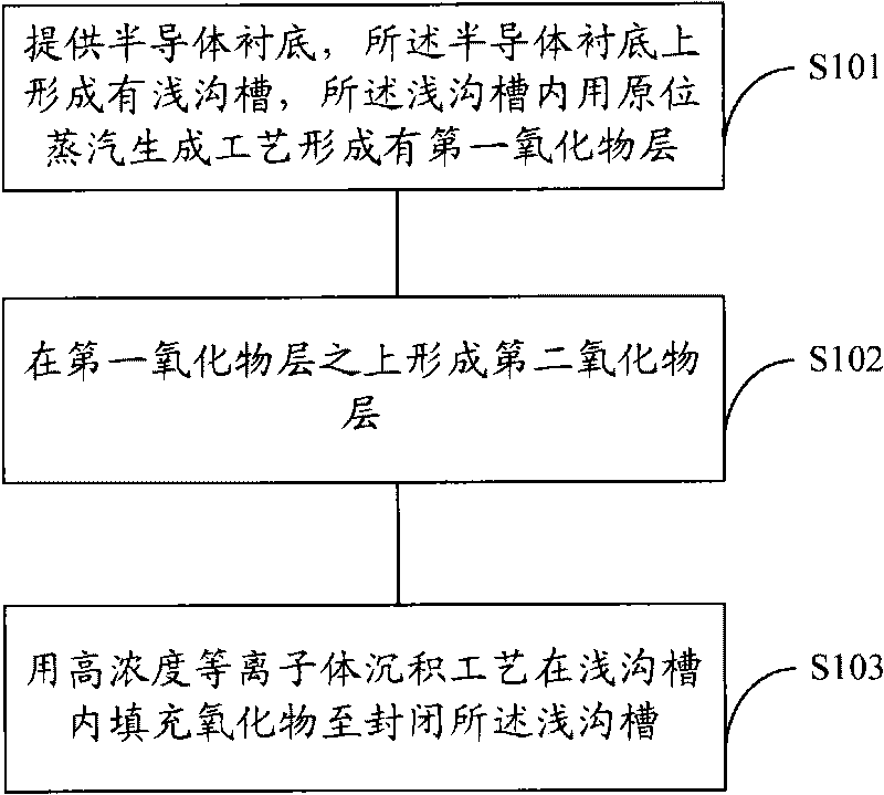
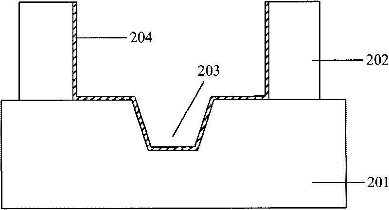
[0020] Narrow Width Effect (Narrow Width Effect) is an important factor affecting the electrical performance of flash memory. The narrow width effect is due to the STI edge geometry, stress, and non-uniform doping distribution along the channel width. These effects have a great influence on the device current, so that the difference of MOS drive current can reach 30%, and the difference of turn-off current can be more than two times.

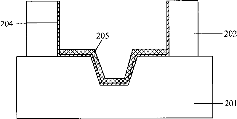
[0021] In order to reduce the narrow width effect, those skilled in the art usually use the ISSG method to form a thin and loose oxide layer in the STI trench of the flash memory structure, that is, the ISSG oxide layer, which is used to repair the substrate crystal in the STI trench. The lattice defects and the improvement of the substrate surface stress in the trench can also protect the substrate surface in the trench and prevent the substrate from being damaged by the subsequent filling process.

[0022] However, when HDP is used to fill th...


PUM


Abstract

The invention relates to a manufacturing method of a shallow trench structure and a flash memory, wherein the manufacturing method of the shallow trench structure comprises the following steps of: providing a semiconductor substrate, forming a shallow trench on the semiconductor substrate and forming a first oxide layer in the shallow trench according to an in-situ steam generation method; forming a second oxide layer on the first oxide layer; and filling an oxide in the shallow trench until closing the shallow trench through a high concentration plasma-chemical vapor deposition process. Compared with the prior art, a high temperature oxide layer is additionally deposited on an ISSG (In-Situ Steam Generation) oxide layer in the shallow trench in the flash memory, the ISSG oxide layer can be protected from being damaged when the shallow trench is filled, the stress environment in the shallow trench can be improved, and the defects in the shallow trench can be repaired, thereby improving the electrical performance of the flash memory.

Description

technical field [0001] The invention relates to the manufacturing field of semiconductor devices, in particular to a shallow trench structure manufacturing method and a flash memory formed therefrom. Background technique [0002] At present, flash memory (Flash), also called flash memory, has become the mainstream of non-volatile memory. According to different structures, flash memory can be divided into two types: NOR Flash and NAND Flash. Among them, non-flash memory is suitable for applications such as mobile phones or motherboards that need to record system codes because of its fast reading speed. And non-flash memory is especially suitable for multimedia data storage because of its high density and high writing speed. Especially in recent years, non-flash memory has been evolving at an annual density doubling rate. The latest generation of NAND flash memory technology has reached a high capacity level of 32Gb per die. In terms of technology, flash memory can be divi...

Claims


Application Information

Patent Timeline
Patent Type & Authority Applications(China)
IPC IPC(8): H01L21/762H01L27/115
Inventor 蔡建祥陈清
Owner SEMICON MFG INT (SHANGHAI) CORP
Why Eureka
Try Eureka