SOI substrate-based antifuse unit structure and preparation process thereof

A preparation process and anti-fuse technology, which is applied in the direction of electrical components, semiconductor/solid-state device manufacturing, semiconductor/solid-state device parts, etc., can solve the problem that the peripheral circuit does not have the advantage of anti-radiation, and the anti-radiation advantage of the anti-fuse unit cannot be obtained Fully embodies other issues, to achieve the effect of enhancing the ability to resist total dose radiation, good resistance to single particle ability, and good resistance to total dose radiation

Active Publication Date: 2011-11-09
WUXI ZHONGWEI JINGYUAN ELECTRONIC CO LTD +1
View PDF0 Cites 3 Cited by
  • Summary
  • Abstract
  • Description
  • Claims
  • Application Information

AI Technical Summary

Problems solved by technology

[0004] Antifuse circuits based on bulk silicon, such as antifuse PROM, FPGA, etc., although antifuse memory cells have strong radiation resistance, the peripheral circuits do not have radiation resistance advantages compared with conventional circuits, so The anti-radiation advantages of the anti-fuse unit cannot be fully reflected

Method used


Image

  • SOI substrate-based antifuse unit structure and preparation process thereof
  • SOI substrate-based antifuse unit structure and preparation process thereof
  • SOI substrate-based antifuse unit structure and preparation process thereof

Examples


Embodiment Construction

[0028] The present invention will be further described below in conjunction with specific drawings and embodiments.

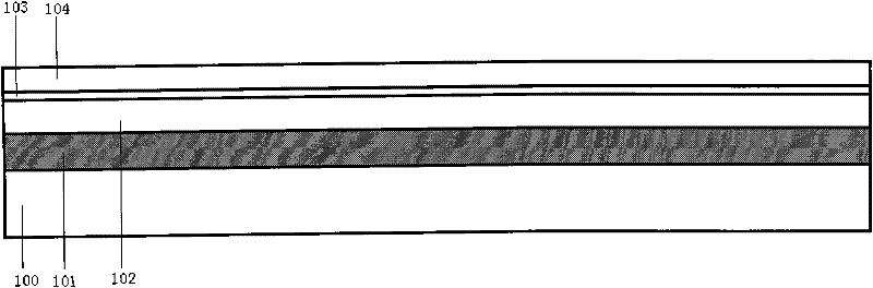
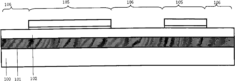
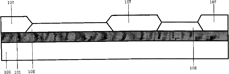
[0029] Figure A-1 to Figure A-8 Description of the identification numbers on the middle picture: 100-bulk silicon substrate, 101-silicon dioxide buried layer, 102-silicon film, 103-third silicon dioxide layer, 104-second silicon nitride layer, 105-first organic Source region, 106-field region, 107-silicon dioxide spacer layer, 108-second active region, 109-MOSFET well region, 110-antifuse lower plate, 111-first silicon dioxide layer, 112- First silicon nitride layer, 113-second silicon dioxide layer, 114-polysilicon layer, 115-silicide layer, 116-MOSFET gate, 117-antifuse upper plate, 118-MOSFET source , 119-MOSFET drain.

[0030] Such as Figure A-8 As shown: the silicon dioxide buried layer 101 is located on the bulk silicon substrate 100, and at least one MOSFET well region 109 and at least one antifuse lower plate 110 are arranged on the silicon dioxide...


PUM


Abstract

The invention relates to an SOI substrate-based antifuse unit structure and a preparation process thereof. The SOI substrate-based antifuse unit structure comprises a bulk silicon substrate and a buried layer of silicon dioxide positioned on the bulk silicon substrate, wherein the buried layer of the silicon dioxide is at least provided with an MOSFET well region and at least one lower polar plate of the antifuse; the MOSFET well region is separated from the lower polar plate of the antifuse through a silicon dioxide spacer layer; a first silicon dioxide layer, a first silicon nitride layer and a second silicon dioxide layer are grown on both of the MOSFET well region and the lower polar plate of the antifuse; the first silicon dioxide layer, the first silicon nitride layer and the secondsilicon dioxide layer respectively serve as a gate medium of the MOSFET and a high-resistance medium of the antifuse; a polycrystalline silicon layer and a silicide layer are distributed on the second silicon dioxide layer orderly; the corresponding polycrystalline silicon layer and the silicide layer on the MOSFET well region serve as the grid of the MOSEFET; the corresponding polycrystalline silicon layer and the silicide layer in a lower polar plate region of the antifuse serve as an upper polar plate of the antifuse; and the MOSFET well region is provided with a source and a drain of the MOSFET. The SOI substrate-based antifuse unit structure has the characteristics of simple process, good compatibility and good radiation resistance performance.

Description

technical field [0001] The invention relates to an anti-fuse unit structure and a preparation process, in particular to an anti-fuse unit structure and a preparation process based on an SOI substrate. Background technique [0002] Antifuse technology has been widely used today, mainly used in PROM, FPGA, PAL and other circuits based on antifuse, and is the most effective solution for one-time programming memory. The antifuse cell has a high-resistance characteristic in the unprogrammed state, with a typical value greater than 10 9 Ω, after programming, it has low-resistance characteristics, and the resistance value is generally less than 200Ω. The deeper meaning is that the anti-fuse-based devices show very good radiation resistance, which makes them well used in military and space fields. [0003] The basic structure of the antifuse unit is a sandwich structure. Both the top layer and the bottom layer are conductive plates, which can be metal, highly doped polysilicon or ...

Claims


Application Information

Patent Timeline
Patent Type & Authority Patents(China)
IPC IPC(8): H01L27/088H01L23/525H01L23/552H01L21/84H01L21/768
CPCH01L2924/0002H10B20/20H01L2924/00
Inventor 洪根深肖志强高向东
Owner WUXI ZHONGWEI JINGYUAN ELECTRONIC CO LTD
Why Eureka
Try Eureka