A silicon-on-insulator material and its reinforcement method against total dose radiation

A technology of silicon-on-insulator and anti-total dose, which is applied in the field of semiconductor technology, can solve the problems of implantation damage, affecting the electrical characteristics of SOI devices and circuits, etc., and achieve the effect of suppressing net accumulation and improving the ability of anti-total dose radiation

Active Publication Date: 2021-05-04
INST OF MICROELECTRONICS CHINESE ACAD OF SCI
View PDF6 Cites 0 Cited by
  • Summary
  • Abstract
  • Description
  • Claims
  • Application Information

AI Technical Summary

Problems solved by technology

This kind of strengthening method is characterized by doping and modifying the material buried layer by means of ion implantation technology. Since the selected impurity elements are implanted into the buried layer through the top silicon film of the SOI material for modification and doping, it is inevitable It will cause implant damage to the top silicon of the SOI material, and will directly affect the electrical characteristics of SOI devices and circuits prepared in the top silicon

Method used


Image

  • A silicon-on-insulator material and its reinforcement method against total dose radiation
  • A silicon-on-insulator material and its reinforcement method against total dose radiation
  • A silicon-on-insulator material and its reinforcement method against total dose radiation

Examples


Embodiment 1

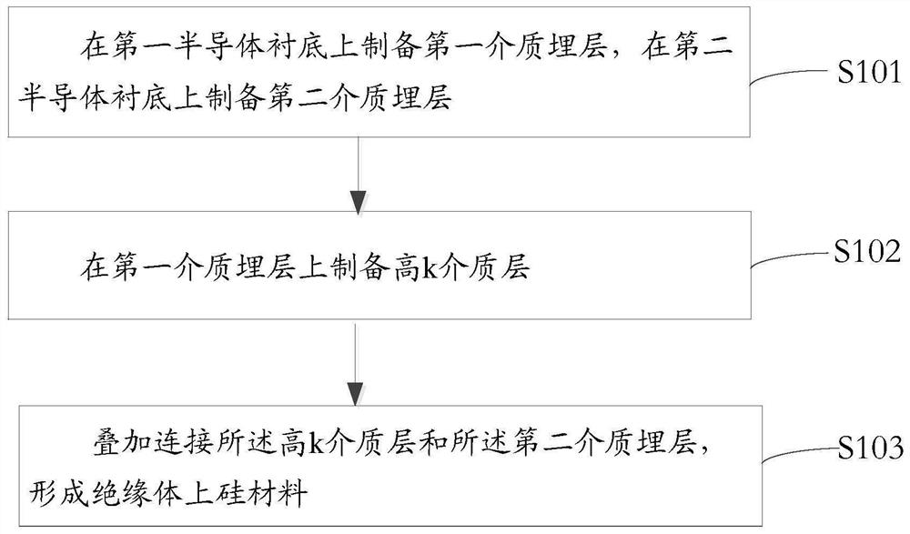
[0033] In this embodiment, a method for strengthening silicon-on-insulator materials against total dose radiation is provided, such as Figure 1~3 shown, including:

[0034] Step S101, preparing a first buried dielectric layer 2 on the first semiconductor substrate 1, and preparing a second buried dielectric layer 4 on the second semiconductor substrate 3;

[0035] Step S102, preparing a high-k dielectric layer 5 on the first buried dielectric layer 2;

[0036] Step S103, superimposingly connecting the high-k dielectric layer 5 and the second buried dielectric layer 4 to form a silicon-on-insulator material.

[0037] It should be noted that step S102 may be performed before the second buried dielectric layer 4 is prepared on the second semiconductor substrate 3, or after or simultaneously with the second buried dielectric layer 4 prepared on the second semiconductor substrate 3, No limitation is imposed here.

[0038] Below, combine Figure 1 ~ Figure 3 , introducing in de...

Embodiment 2

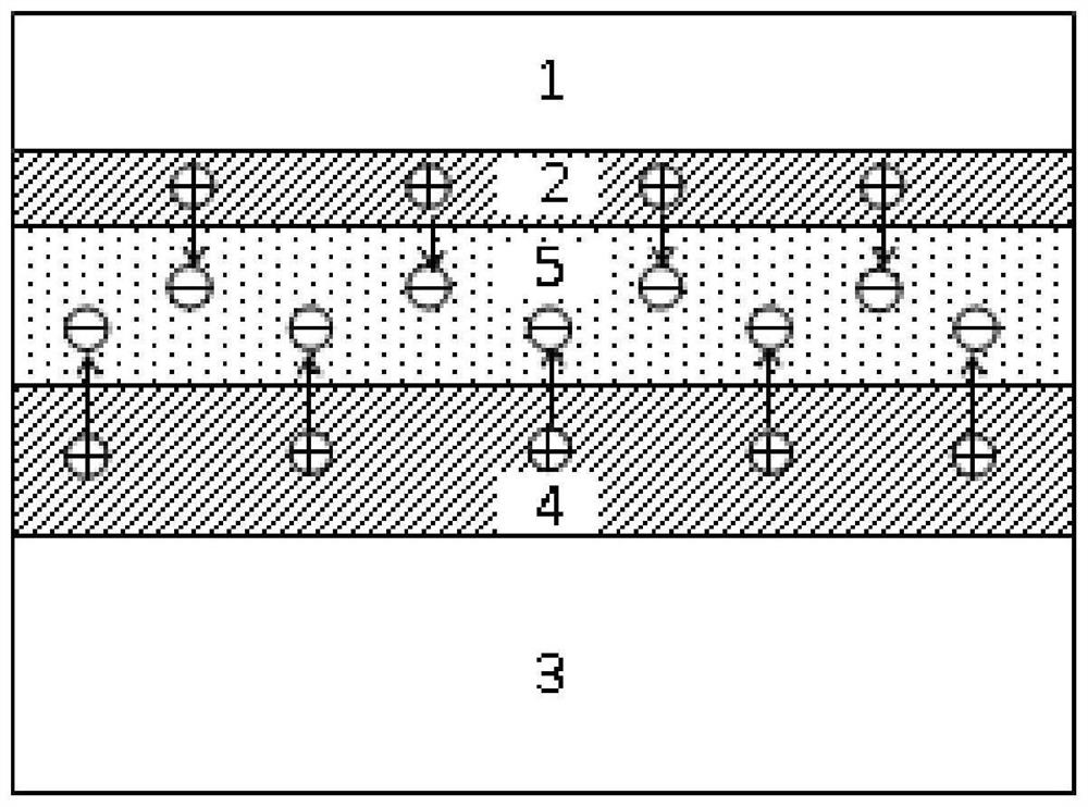
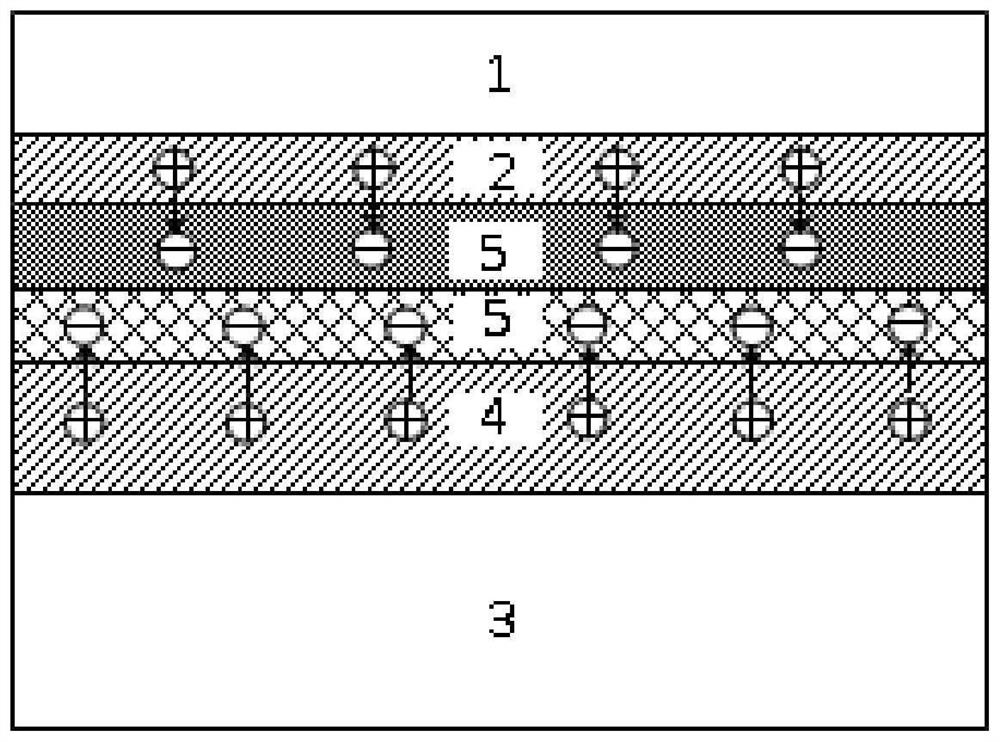
[0057] This embodiment provides a silicon-on-insulator material, such as figure 2 and 3 shown, including:

[0058] The first semiconductor layer 1, the first buried dielectric layer 2, the second buried dielectric layer 4 and the second semiconductor layer 3 stacked in sequence;

[0059] Wherein, a high-k dielectric layer 5 is embedded between the first buried dielectric layer 2 and the second buried dielectric layer 4 .

[0060] In the embodiment of the present application, the theoretical total trapped charge density value of the first buried dielectric layer 2, the second buried dielectric layer 4 and the high-k dielectric layer 5 tends to zero under preset working conditions.

[0061] In the embodiment of the present application, the high-k dielectric layer 5 includes a high-k material with an initial negative charge for electron traps.

[0062] In the embodiment of the present application, the high-k dielectric layer 5 includes multiple high-k dielectric layers of dif...


PUM

PropertyMeasurementUnit
relative permittivityaaaaaaaaaa

Abstract

The invention discloses a silicon-on-insulator material and a method for strengthening it against total dose radiation. The method comprises: preparing a first dielectric buried layer on a first semiconductor substrate, and preparing a second dielectric buried layer on a second semiconductor substrate; A high-k dielectric layer is prepared on the first dielectric buried layer; the high-k dielectric layer and the second dielectric buried layer are stacked and connected to form a silicon-on-insulator material. The invention provides a silicon-on-insulator material and a method for strengthening it against total dose radiation, thereby avoiding damage to the top-layer semiconductor material while realizing radiation reinforcement.

Description

technical field [0001] The invention relates to the technical field of semiconductor technology, in particular to a silicon-on-insulator material and a method for strengthening it against total dose radiation. Background technique [0002] Compared with bulk silicon integrated circuits, integrated circuits based on silicon-on-insulator (SOI) technology have the advantages of low power consumption, high speed, high temperature resistance, and latch-up resistance, and are therefore widely used. The advantage of SOI circuits comes from the unique structure that the top layer device is completely isolated from the substrate by the buried insulating layer of SOI material. In particular, the existence of the buried layer reduces the sensitive volume of the device in the single event radiation environment, and significantly enhances the ability of the circuit to resist single event event upset (SEU), making SOI materials the first choice for making highly reliable radiation hardene...

Claims


Application Information

Patent Timeline
Patent Type & Authority Patents(China)
IPC IPC(8): H01L21/762H01L27/12
Inventor 郑中山朱慧平孔延梅李多力李博罗家俊韩郑生焦斌斌
Owner INST OF MICROELECTRONICS CHINESE ACAD OF SCI
Why Eureka
Try Eureka