Anti-radiation high-voltage device structure

A high-voltage device and anti-radiation technology, which is applied in the direction of semiconductor devices, electrical solid devices, semiconductor/solid device components, etc., can solve the problems of on-resistance degradation and other problems, so as to inhibit the degradation of device on-resistance and improve the total anti-dose The effect of radiation ability

Active Publication Date: 2022-07-29
UNIV OF ELECTRONICS SCI & TECH OF CHINA +1
View PDF9 Cites 0 Cited by
  • Summary
  • Abstract
  • Description
  • Claims
  • Application Information

AI Technical Summary

Problems solved by technology

[0003] To solve the problem of on-resistance degradation after total dose radiation of high-voltage LDMOS devices, the invention proposes a radiation-resistant high-voltage device structure

Method used


Image

  • Anti-radiation high-voltage device structure
  • Anti-radiation high-voltage device structure
  • Anti-radiation high-voltage device structure

Examples


Embodiment

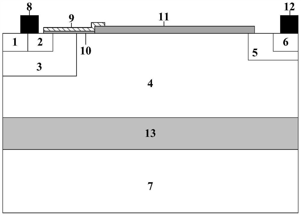
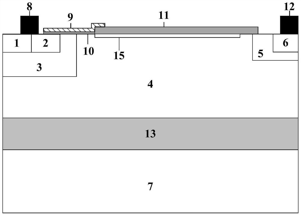
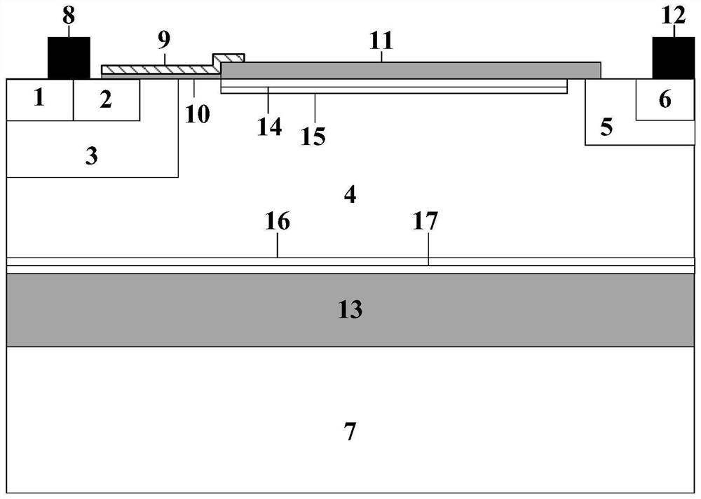
[0023] like image 3 As shown, this embodiment provides a radiation-resistant high-voltage LDMOS device structure, including a first conductive type substrate 7, a buried oxide layer 13 formed on the first conductive type substrate 7, and a buried oxide layer 13 formed on the buried oxide layer 13. The first conductivity type highly doped Pbury+ layer 17 and the first conductivity type generally doped Pbury layer 16, the first conductivity type generally doped Pbury layer 16 is formed on the second conductivity type drift region 4; the first conductivity type well region 3 The first conductive type body region 1 is located in the upper left corner of the second conductive type drift region 4, the first conductive type body region 1 is located in the first conductive type well region 3, and the second conductive type source region 2 is located in the first conductive type well region 3. The right side of the body region 1; the source electrode 8 is placed above the first conduc...


PUM


Abstract

Compared with a traditional high-voltage LDMOS (Laterally Diffused Metal Oxide Semiconductor) device structure, the radiation-resistant high-voltage device structure provided by the invention has the advantages that a highly-doped Ptop + layer and a generally-doped Ptop layer are introduced into a drift region below a field oxide layer; a highly doped Pury + layer and a generally doped Pury layer are introduced into the drift region above the buried oxide layer. According to the invention, the newly introduced highly doped layer can shield the influence of positive radiation trapped charges in the oxide layer on the drift region, and the degradation of the on-resistance of the device caused by the total dose radiation effect is effectively inhibited under the condition of keeping the initial characteristics unchanged.

Description

technical field [0001] The invention belongs to the field of semiconductor power devices, in particular to a radiation-resistant LDMOS high-voltage device structure. Background technique [0002] With the increasing application of power semiconductor devices in aerospace electronic systems, for power management systems and gate drive circuits, radiation hardening technology has become the research focus of various companies and universities. As the core part of the analog circuit, the high-voltage LDMOS device is characterized by occupying a large area and having a larger field oxide layer. Therefore, in the radiation environment such as γ-ray, LDMOS devices are prone to withstand voltage degradation, on-resistance degradation, and threshold drift. In severe cases, the device fails and the entire circuit cannot work normally. Therefore, it is necessary to study radiation-resistant high-voltage LDMOS devices. SUMMARY OF THE INVENTION [0003] To solve the problem that the ...

Claims


Application Information

Patent Timeline
Patent Type & Authority Applications(China)
IPC IPC(8): H01L23/552H01L29/06H01L29/78
CPCH01L29/7816H01L29/0684H01L23/552
Inventor 周锌高聪乔明张波
Owner UNIV OF ELECTRONICS SCI & TECH OF CHINA
Why Eureka
Try Eureka