
Process for total dose radiation hardening of factory region

A radiation-resistant hardening and total dose technology, which is applied in the fields of electrical solid-state devices, semiconductor/solid-state device manufacturing, semiconductor/solid-state device components, etc., can solve the problems of turn-on voltage drift, NMOS field tube turn-on voltage drop, and loss of isolation performance, etc. , to achieve the effects of suppressing the drift of the opening voltage, improving the ability to resist total dose radiation, and strong operability

Active Publication Date: 2013-05-08
58TH RES INST OF CETC
View PDF5 Cites 0 Cited by
  • Summary
  • Abstract
  • Description
  • Claims
  • Application Information

AI Technical Summary

Problems solved by technology

Due to the use of thermal silicon dioxide material as the field isolation medium, a large turn-on voltage drift occurs under the condition of large doses of radiation. The most notable is that the turn-on voltage of the NMOS field tube drops significantly, and even the field tube is fully turned on. Isolation performance

Method used

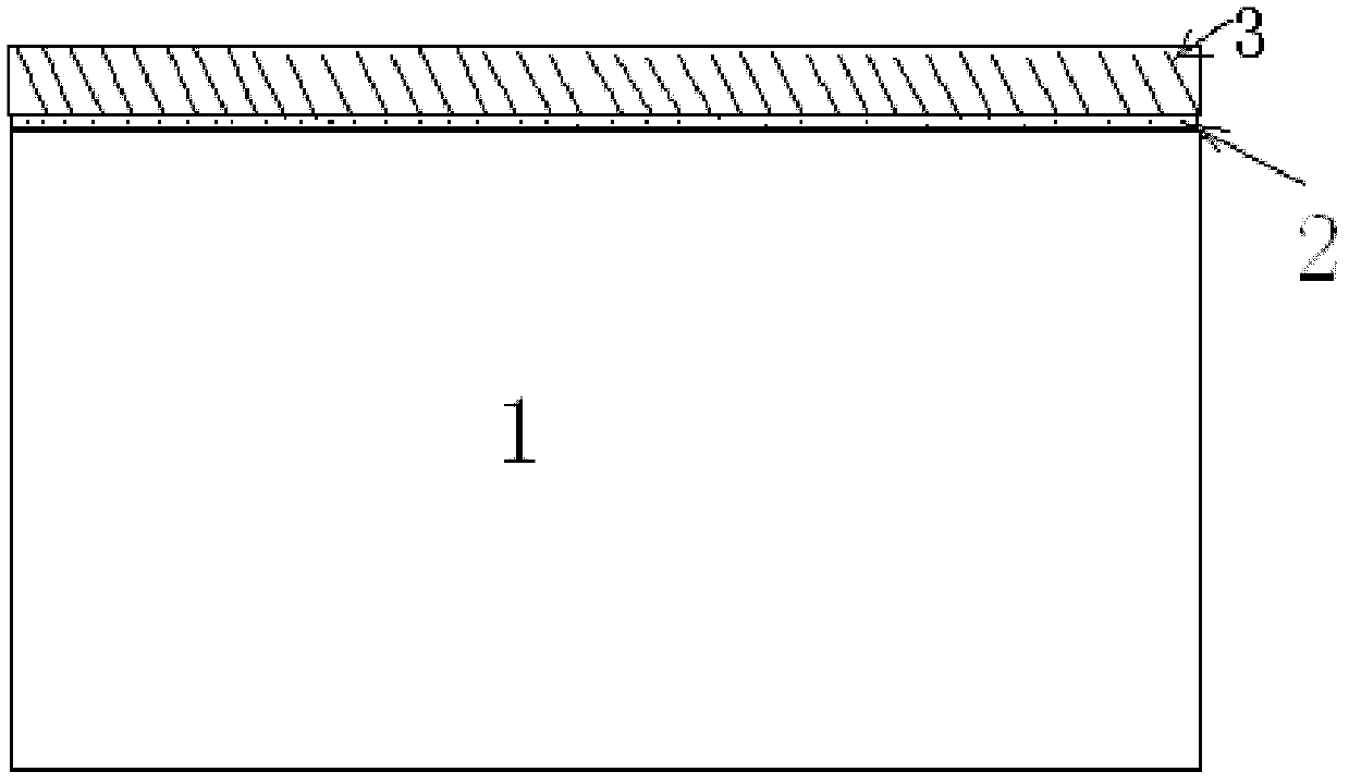
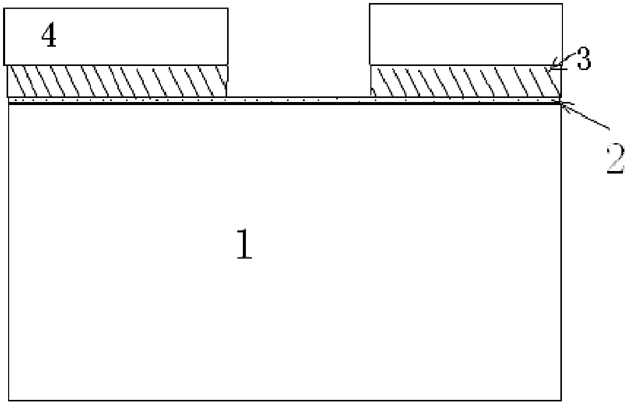
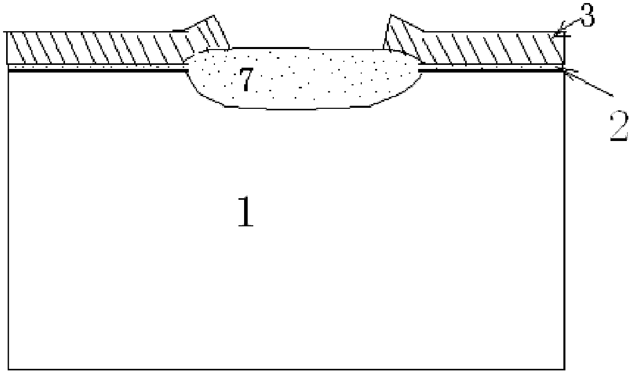

Image

  • Process for total dose radiation hardening of factory region
  • Process for total dose radiation hardening of factory region
  • Process for total dose radiation hardening of factory region

Examples


Embodiment Construction

[0038] The present invention will be further described below in conjunction with specific drawings and embodiments.

[0039] Such as Figure 6~Figure 11 Shown: take the N-type MOS field tube as an example, the present invention comprises the following steps:

[0040] a, providing a substrate 8, and forming a first silicon dioxide layer 9 on the surface of the substrate 8;

[0041] Such as Figure 6 As shown: the substrate 8 is made of P-type silicon material, the first silicon dioxide layer 9 is formed on the substrate 8 by thermal oxidation, the thickness of the substrate 8 is the SEMI standard thickness, and the thickness of the first silicon dioxide layer 9 is 10~40nm;

[0042] b. A composite material layer 11 is provided on the above-mentioned first silicon dioxide layer 9, the composite material layer 11 is formed by interlacing the amorphous silicon material layer 10 and the second silicon dioxide layer, and the composite material layer 11 passes through The amorphou...


PUM

PropertyMeasurementUnit
thicknessaaaaaaaaaa
thicknessaaaaaaaaaa
thicknessaaaaaaaaaa

Abstract

The invention relates to a process for total dose radiation hardening of a factory region, which comprises the following steps of: a, providing a substrate, and forming a first silicon dioxide layer on the surface of the substrate; b, setting a composite material layer on the first silicon dioxide layer; c, etching the composite material layer to form a field isolation structure; d, depositing polycrystalline silicon, and etching the polycrystalline silicon to form a polycrystalline silicon strip on the field; and e, forming polycrystalline silicon strip surface ion implantation on the surface of the substrate to form source and drain heavily doped regions, wherein the source and drain heavily doped regions are located at the two sides of the composite material layer. The process providedby the invention adopts a noncrystalline silicon material layer and a complex material layer formed by depositing a second silicon dioxide layer through PECVD (Plasma Enhanced Chemical Vapor Deposition), has excellent radiation hardening performance and good electric isolation property, and can suppress cut-in voltage drift of an NMOS (N-channel Metal Oxide Semiconductor) field tube under large dose radiation condition and improve total dose radiation hardening capability of an integrated circuit; and the process is simple in processing technology and good in operability.

Description

technical field [0001] The present invention relates to a radiation resistance strengthening process, in particular to a radiation resistance strengthening process for the total field dose, in particular to the field area total dose radiation resistance for bulk silicon CMOS and SOI (silicon on insulator) materials The reinforcement process belongs to the technical field of integrated circuits. Background technique [0002] In integrated circuits, the field region is mainly used for isolation between devices, and the field region is mainly composed of SiO 2 It is composed of dielectric, and multi-stripes pass through the field area. This structure is very similar to the conventional MOS tube structure in integrated circuits. Generally, it can be regarded as a MOS tube structure with the field area dielectric layer as the gate oxide structure. This MOS tube structure is usually called a MOS field tube, which has a high turn-on voltage (generally more than twice the circuit o...

Claims


Application Information

Patent Timeline
Patent Type & Authority Patents(China)
IPC IPC(8): H01L21/336H01L23/552
Inventor 吴建伟肖志强高向东洪根深
Owner 58TH RES INST OF CETC
Learn More