Coupling inductance type double Boost inverter circuits in photovoltaic system

A photovoltaic power generation system and coupled inductor technology, applied in the fields of power electronics and electrical engineering, can solve the problems of large power loss of the power switch tube, affecting the utilization rate of photovoltaic power generation, and low utilization rate of photovoltaic power generation, achieving low design cost and improving comprehensive conversion. Efficiency, low cost effect

Inactive Publication Date: 2010-06-16
SUNHUI NEW ENERGY CO LTD
View PDF0 Cites 26 Cited by
  • Summary
  • Abstract
  • Description
  • Claims
  • Application Information

AI Technical Summary

Problems solved by technology

In the former, when the voltage of the photovoltaic module is low, the step-up ratio of the power frequency transformer is relatively large, and the current of the primary side is relatively large, so the power loss of the power switch tube is relatively large, and the power loss of the transformer itself results in low conversion efficiency of the system, which affects the photovoltaic system. The utilization rate of power generation; in the latter, a two-stage circuit is used, and the conversion efficiency of the system is not high, resulting in a low utilization rate of photovoltaic power generation
It can be seen that these two methods are not conducive to the efficient power generation of medium and low-power photovoltaic cells under low-voltage photovoltaic modules to the grid.

Method used


Image

  • Coupling inductance type double Boost inverter circuits in photovoltaic system
  • Coupling inductance type double Boost inverter circuits in photovoltaic system
  • Coupling inductance type double Boost inverter circuits in photovoltaic system

Examples


Embodiment Construction

[0046] The specific embodiment, working principle and working process of the present invention are described according to the above drawings.

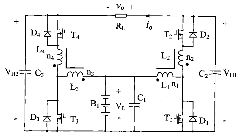
[0047] Such as figure 1 Shown, the coupled inductance boost inverter circuit is made up of the present invention by following parts:

[0048] Coupled inductor L 1 , L 2 , coupled inductance L 3 , L 4 , input DC source B 1 and its parallel capacitance C 1 , switch tube T 1 ~T 4 and its antiparallel diode D 1 ~D 4 , output filter capacitor C 2 , C 3 and simulated load R Lcomposition.

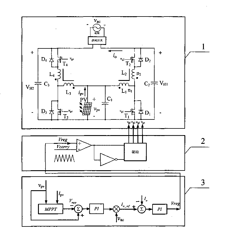
[0049] figure 1 is the main circuit of the present invention, figure 2 yes figure 1 An application system, the connection of the inverter is also the main content of the present invention.

[0050] Such as figure 2 Shown:

[0051] Inverter 1 (coupled inductive Boost inverter), modulator 2 (SPWM bipolar modulator) and controller 3 (controller with MPPT) form the application of the present invention; wherein, the output of controller 3 i...


PUM


Abstract

The invention relates to coupling inductance type double-Boost inverter circuits in a photovoltaic system, which comprises two coupling inductance type Boost circuits sharing a direct current power supply, and alternate current output is taken from two coupling inductance type Boost output capacitors. The invention solves the defects of large power loss of a power switching tube, large power loss of a transformer, low conversion efficiency, low utilization rate of photovoltaic generation and the like in a method in which a single-stage inversion circuit is combined to the grid through an industrial frequency transformer boost mode, a DC-DC boosted circuit is at the front stage and an inverter is at the back stage. The invention comprises two coupling inductance type Boost circuits and uses a full-control type device switching tube, so the inversion circuit can realize four-quadrant operation of energy; and under the conditions that the coupled inductance has lower input voltage and smaller duty ratio, the Boost circuits can also output higher voltage, thus the grid-combined inverter of the invention does not need a booster transformer and can realize primary grid-combined generation.

Description

technical field [0001] The invention belongs to the technical field of power electronics and electric engineering, and in particular relates to a coupled inductance double Boost inverter circuit in a photovoltaic power generation system. Background technique [0002] Prior to the present invention, the existing low-voltage DC inverter technology, especially in the grid-connected power generation of low-voltage photovoltaic modules, mainly includes the following two types. [0003] One is a single-stage inverter circuit connected to the grid through a power frequency transformer step-up method, and the other is a two-stage type, that is, the front-stage DC-DC step-up circuit, and the rear stage is an inverter. In the former, when the voltage of the photovoltaic module is low, the step-up ratio of the power frequency transformer is relatively large, and the current of the primary side is relatively large, so the power loss of the power switch tube is large, and the power loss ...

Claims


Application Information

Patent Timeline
Patent Type & Authority Applications(China)
IPC IPC(8): H02M7/537H02J3/38
CPCY02E10/563Y02E10/56
Inventor 方宇
Owner SUNHUI NEW ENERGY CO LTD
Why Eureka
Try Eureka