Impedance adjusting device and impedance matching system comprising same
A technology of impedance adjustment and impedance matching, which is applied in the direction of impedance network, electrical components, multi-terminal pair network, etc., can solve problems such as difficulty in matching network, and achieve the effect of avoiding power loss
- Summary
- Abstract
- Description
- Claims
- Application Information
AI Technical Summary
Problems solved by technology
Method used
Image

Examples
Embodiment 1
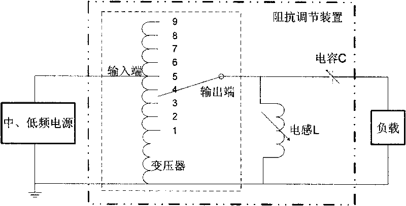
[0035] refer to image 3 , is a schematic diagram of a mid- and low-frequency impedance matching system described in Embodiment 1 of the present invention.
[0036] The system mainly includes medium and low frequency power supplies, an impedance adjustment device (dotted line in the figure) and a load. Wherein, the impedance adjusting device includes a transformer and a capacitor C, the input end of the transformer is connected to the medium and low frequency power supply, and the output end of the transformer is connected to the capacitor C. Wherein, the capacitor C may be a fixed capacitor or an adjustable capacitor.
[0037] The present invention does not limit the type of the transformer. In this embodiment, the transformer is an isolation transformer composed of primary and secondary. The primary of the isolation transformer is connected to the medium and low frequency power supply. The secondary of the isolation transformer is connected to the capacitor C and The above...
Embodiment 2
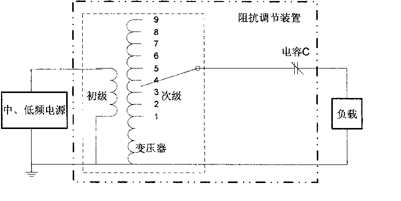
[0043] refer to Figure 4 , is a schematic diagram of a mid- and low-frequency impedance matching system described in Embodiment 2 of the present invention.
[0044] The system mainly includes medium and low frequency power supplies, an impedance adjustment device (dotted line in the figure) and a load. Wherein, the impedance adjusting device includes a transformer, a capacitor C and an inductor L, the input end of the transformer is connected to the medium and low frequency power supply, and the output end of the transformer is connected with the capacitor C and the inductor L.
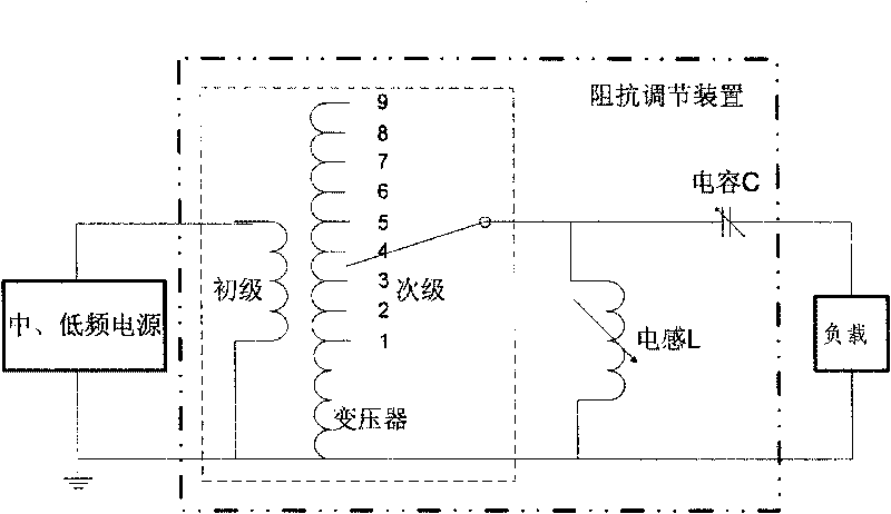
[0045] The present invention does not limit the type of the transformer. In this embodiment, the transformer is an isolation transformer composed of a primary and a secondary. The primary of the isolation transformer is connected to the medium and low frequency power supply, and the secondary of the isolation transformer is connected to the inductance L first. It is then sequentially connected with ...
Embodiment 3
[0058] Embodiment 3 provides an impedance matching device with a transformer different from Embodiment 2.
[0059] refer to Figure 5 , is a schematic diagram of a mid- and low-frequency impedance matching system described in Embodiment 3 of the present invention.
[0060] The system mainly includes medium and low frequency power supplies, an impedance adjustment device (dotted line in the figure) and a load. Wherein, the impedance adjustment device includes an autotransformer, a capacitor C and an inductance L, the input end of the autotransformer is connected with the medium and low frequency power supply, the output end of the autotransformer is first connected with the inductance L, and then connected with the The capacitor C and the load are sequentially connected to form a path. Of course, the inductor L can be connected in parallel with the capacitor C and the load (such as Figure 5 shown), the inductor L can also be connected in series with the capacitor C and the ...
PUM
 Abstract
Description
Claims
Application Information
PatSnap Eureka turns technology decisions into work you can execute. Powered by our Innovation Knowledge Graph, it runs expert workflows across engineering, life sciences, materials and intellectual property. Get your review-ready output in minutes.


