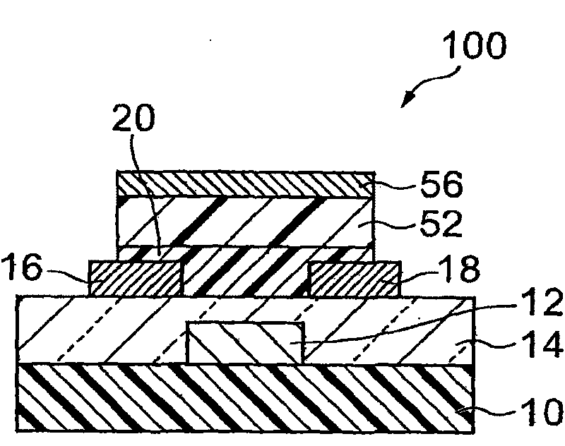
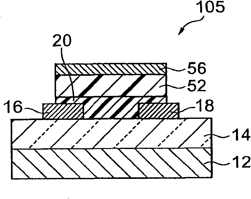
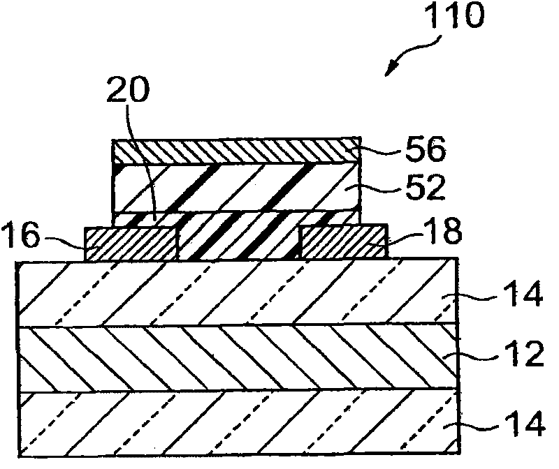
Process for producing organic semiconductor element, organic semiconductor element, and organic semiconductor device

A technology for organic semiconductors and manufacturing methods, which is applied in the fields of semiconductor/solid-state device manufacturing, semiconductor devices, electrical components, etc., can solve the problems of deterioration of the active layer, difficulty in fine and good pattern shape, etc., and achieves a minimal reduction effect.

Inactive Publication Date: 2010-06-16
SUMITOMO CHEM CO LTD
View PDF3 Cites 1 Cited by
  • Summary
  • Abstract
  • Description
  • Claims
  • Application Information

AI Technical Summary

Problems solved by technology

A method of providing a protective layer to protect the active layer is also considered, but in this case, not only the deterioration of the active layer due to the formation of the protective layer, but also the influence on the orientation must be considered.
Thus, in the case of forming an oriented active layer, it tends to become more difficult to form a fine and good pattern shape.

Method used


Image

  • Process for producing organic semiconductor element, organic semiconductor element, and organic semiconductor device
  • Process for producing organic semiconductor element, organic semiconductor element, and organic semiconductor device
  • Process for producing organic semiconductor element, organic semiconductor element, and organic semiconductor device

Examples


Embodiment 1

[0174] (manufacturing of transistors)

[0175] Next, a transistor is manufactured based on the transistor manufacturing method of the third embodiment described above. Figure 21 , 22 23 and 23 are diagrams showing the manufacturing process of the transistor of the first embodiment. First, if Figure 21 As shown in (a), a highly doped n-type silicon substrate 1 serving as a gate electrode and a substrate is prepared, and its surface is thermally oxidized to form a 200nm silicon oxide film to be an insulating layer 3 . Next, if Figure 21 As shown in (b), a 50nm-thick gold was evaporated on the surface of one insulating layer 3 of the substrate 1 by a vacuum evaporation method to form a source electrode 4a and a drain electrode 4b having lead lines and pads. The electrode at this time had a channel width of 500 μm and a channel length of 40 μm.

[0176] Next, according to the method described in the literature (S.R.Wasserman, et al., Langmuir, Vol.5, p1074, 1989), by immer...

Embodiment 2

[0185] (manufacturing of transistors)

[0186] In Example 2, a transistor including an active layer including poly(3-dodecylthiophene) was produced by performing the same steps as in Example 1 except for the following changes. That is, the points changed from Example 1 are: (a) the channel length is 200 μm instead of 40 μm; processing; (c) as a material for forming the semiconductor film 8, a chloroform solution of poly(3-dodecylthiophene) was used instead of a chlorobenzene solution of poly(3-hexylthiophene); (d) the support film 7 was replaced by A poly(1-methylpentene) film is replaced by a polyethylene film that has not been subjected to oxygen plasma treatment; (e) the condition of the stretching operation of the laminate 5 is replaced by 4 times of uniaxial stretching at 175° C., Uniaxially stretched 5 times at 100°C; (f) when forming the mask layer 156, the drying of the solution of polyvinyl alcohol was replaced by heat treatment at 80°C for 1 hour, and at 70°C for 1 ...


PUM


Abstract

This invention provides a process for producing an organic semiconductor element which can prevent a lowering in electrical characteristics of an active layer and, at the same time, can form an active layer which has been patterned so as to form a good pattern shape. The production process comprises the step of applying a laminate of a support film stacked on an active layer onto an element substrate on which an active layer is to be formed, so that the active layer in the laminate comes into contact with the element substrate, the step of forming a mask having a predetermined pattern shape on a support film on its side remote from the active layer, and the step of removing the laminate in its region free from the mask to pattern an active layer.

Description

technical field [0001] The present invention relates to a method for manufacturing an organic semiconductor element, an organic semiconductor element obtained by the method, and an organic semiconductor device including the organic semiconductor element. Background technique [0002] An organic semiconductor element is an element having an active layer including a semiconductor film containing an organic semiconductor compound. Examples of such organic semiconductor elements include transistors, circuit elements, and the like, and these are applied to semiconductor devices such as displays, for example. When applying an organic semiconductor element to a semiconductor device, it is necessary to form the active layer into a pattern having a shape corresponding to a circuit pattern formed on the semiconductor device. [0003] As a method of forming a patterned active layer in an organic semiconductor element, as in the conventional inorganic semiconductor element, a photoresi...

Claims


Application Information

Patent Timeline
IPC IPC(8): H01L21/336H01L29/786H01L51/05H01L51/40
CPCH01L51/0012H01L51/0002H01L51/0018H01L51/0545H01L51/0541H01L51/057H01L51/0013H01L51/0024H01L51/003H10K71/10H10K71/191H10K71/18H10K71/233H10K71/50H10K71/80H10K10/464H10K10/491H10K10/466H10K71/20
Inventor 山手信一
Owner SUMITOMO CHEM CO LTD
Why Eureka
Try Eureka