CIS solar cell and method for manufacturing the cis solar cell

A technology of solar cells and manufacturing methods, applied in the direction of final product manufacturing, sustainable manufacturing/processing, circuits, etc., can solve problems such as poor light utilization effect, and achieve high productivity and improve conversion efficiency.

Active Publication Date: 2010-06-16
ORMON CORP
View PDF1 Cites 4 Cited by
  • Summary
  • Abstract
  • Description
  • Claims
  • Application Information

AI Technical Summary

Problems solved by technology

Therefore, there is a problem that the light cannot be sufficiently scattered by the lower ele

Method used


Image

  • CIS solar cell and method for manufacturing the cis solar cell
  • CIS solar cell and method for manufacturing the cis solar cell
  • CIS solar cell and method for manufacturing the cis solar cell

Examples


no. 1 approach

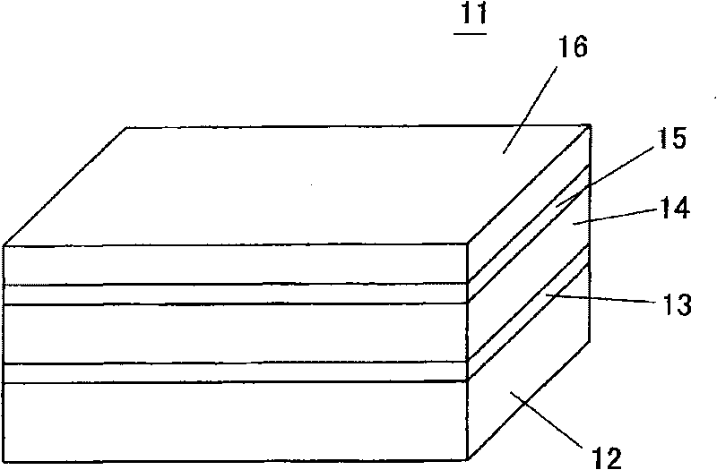
[0050] Below, refer to Figure 4 The structure of the CIS-based solar cell 31 according to the first embodiment of the present invention will be described. In this CIS-based solar cell 31, a CIS-based (chalcopyrite compound-based) light-absorbing layer 33 such as CIGS, CIGSS, or CIS is formed on an alloy substrate 32 produced by electroforming, and a transparent layer 33 is formed thereon via a buffer layer 34. The upper electrode 35. In addition, a pair of extraction electrodes 36 are provided on the upper surface of the upper electrode 35 . As a typical example, the alloy substrate 32 is an alloy of Ni and Mo, and has a thickness of about 50 μm. The light absorbing layer 33 is formed of CIGS to have a thickness of 2 μm to 3 μm. The buffer layer 34 is formed of CdS or the like to a thickness of 0.05 μm (50 nm) to 0.1 μm (100 nm). The upper electrode 35 is formed of ZnO or the like to a thickness of 0.6 μm (600 nm).

[0051] The alloy substrate 32 is an alloy of Ni and Mo...

no. 2 approach

[0069] Next, a second embodiment of the present invention will be described. Since the structure of the CIS-based solar cell is the same as that of the first embodiment, illustration and description thereof will be omitted.

[0070] In the first embodiment, the alloy substrate 32 is an alloy of Mo and Ni, but in the second embodiment, the alloy substrate 32 is made using an alloy of Mo and Co. In this case, the lower surface is made of Co, and the upper surface on which the concavo-convex shape 37 is formed is a Mo layer or a high-Mo alloy layer. In the case of this Mo-Co alloy, as Figure 9 As shown in (a) and (b), the Mo concentration in the film is also changed by the Mo concentration in the solution and the current density. Therefore, in the electroforming process, by changing the current density and the Mo concentration in the solution, the alloy substrate 32 can be changed. Mo concentration.

[0071] In order to make the linear expansion coefficient of the alloy subst...

no. 3 approach

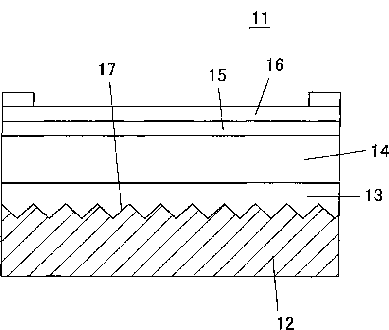
[0074] Figure 10 It is a perspective view of an alloy substrate 32 used in a CIS-based solar cell according to a third embodiment of the present invention. In this alloy substrate 32, as Figure 10 As shown, the upper surface of the alloy substrate 32 is provided with minute triangular groove-shaped concave-convex shapes 37 . In such a triangular groove-like concave-convex shape 37 , light can also be scattered, thereby improving the conversion efficiency of the CIS-based solar cell.


PUM

PropertyMeasurementUnit
Thicknessaaaaaaaaaa
Thicknessaaaaaaaaaa
Thicknessaaaaaaaaaa

Abstract

An alloy substrate (32) formed of an alloy of Ni and Mo is formed by electroforming. The alloy substrate (32) has a graded composition with an alloy composition varied in its thickness direction. In this case, the alloy substrate (32) on its lower surface side is mainly composed of Ni, and the alloy substrate (32) on its upper surface side is mainly composed of Mo. The alloy substrate (32) has on its upper surface a large number of minute pyramid-shaped concavoconvexes (37) with a high light scattering effect. A CIS optical absorption layer (33) is provided on the upper surface of the alloy substrate (32), and an upper electrode (35) is provided above the optical absorption layer (33).

Description

technical field [0001] The present invention relates to a CIS-based solar cell and a manufacturing method thereof, and more specifically, to a CIS-based solar cell using CIGS, CIGSS, CIS, or the like as a light absorbing layer, and to a manufacturing method thereof. Background technique [0002] In solar cells, there are monocrystalline silicon solar cells, polycrystalline silicon solar cells, amorphous silicon solar cells (the above are all silicon-based solar cells), GaAs-based solar cells, CdS / CdTe-based solar cells, and CIS-based solar cells. (All of the above are compound-based solar cells), dye-sensitized solar cells (organic-based), etc. [0003] Among them, CIS-based solar cells have the following characteristics: they are multi-crystalline and are suitable for large-area and mass production, and the bandgap width can be freely changed depending on the material, and have a theoretical conversion efficiency equivalent to that of silicon-based solar cells. (31%), and ...

Claims


Application Information

Patent Timeline
IPC IPC(8): H01L31/04C25D1/00
CPCH01L31/0236H01L31/0749C25D3/562C25D1/04Y02E10/50H01L31/0392Y02E10/541H01L31/02366H01L31/03923H01L31/03925Y02E10/52Y02P70/50H01L31/056
Inventor 大田盛久小林大造船本昭宏青山茂
Owner ORMON CORP
Why Eureka
Try Eureka