Method of layout design of laterally diffused MOS transistor

A MOS transistor and layout design technology, applied in transistors, computing, electrical solid devices, etc., can solve the problems of large drain resistance, difficult resistance value, large drain area, etc., to reduce parasitic resistance, increase uniformity, The effect of even wiring

Inactive Publication Date: 2010-06-23
SHANGHAI HUA HONG NEC ELECTRONICS
View PDF0 Cites 12 Cited by
  • Summary
  • Abstract
  • Description
  • Claims
  • Application Information

AI Technical Summary

Problems solved by technology

The current direction of the transistor array designed with this structure is fixed, generally only the current along the cross-sectional direction, and the optimization of the array area cannot be realized
Due to the large drain area of ​​conventional LDMOS, the junction depth also includes the drift region, so the drain resistance is large, and it is difficult to improve its resistance through technological means
At the same time, the arrangement of LDMOS transistors with an interdigitated structure cannot achieve uniform wiring.

Method used


Image

  • Method of layout design of laterally diffused MOS transistor
  • Method of layout design of laterally diffused MOS transistor
  • Method of layout design of laterally diffused MOS transistor

Examples


Embodiment Construction

[0016] In the layout design method of the laterally diffused MOS transistor of the present invention, there are mainly the designs of the following areas:

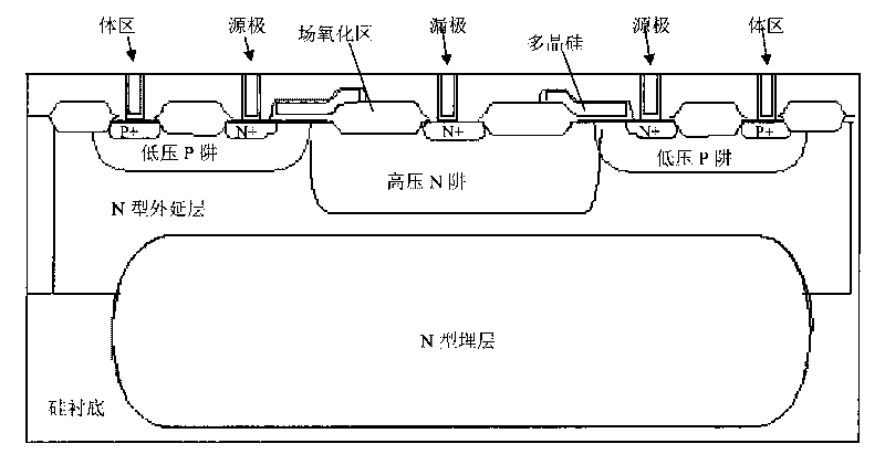
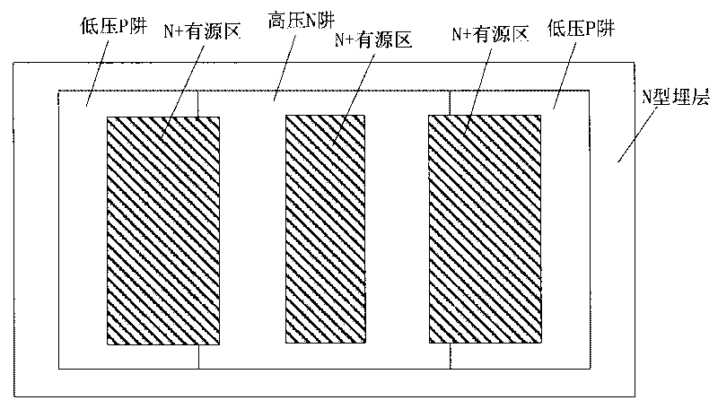
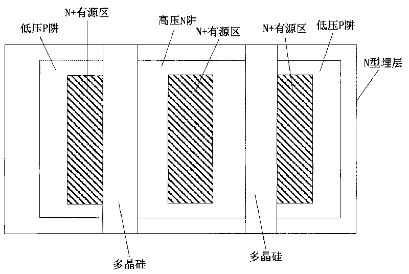
[0017] 1. The design method of the well is: usually LDMOS transistors use low-voltage or high-voltage wells as the source and drain regions to increase the breakdown voltage. In the design method of the present invention, the design of the well adopts a grid-like layout to ensure that each source region is surrounded by a drain region, and each drain region is also surrounded by a source region. image 3 In order to adopt the design method of a single unit of the source region and the drain region in the method of the present invention, it is formed by splicing two LDMOS transistors, the high-voltage N well region is the drain region, the P well region is the source region, and the source region and the drain region are phase Adjacent squares form a 3×3 square array unit (see Figure 4 ). By splicing and arranging a plur...


PUM


Abstract

The invention discloses a method of a layout design of a laterally diffused MOS transistor, which adopts the grid-shaped layout design and designs wells of a source region and a drain region of the laterally diffused MOS transistor in square shape, each well as the source region is surrounded by the well as the drain region, and each well as the drain region is surrounded by the well as the source region at the same time, then a square region with a smaller side length is defined as an active region of the drain region in the square of the well as the drain region, the well as the source region and a thin oxide layer defining region of the drain region are acted as an active region, and the rest annular part of the well as the drain region is acted as a field oxide region, polycrystalline silicon is arranged at the connecting part of the square of the source region and the square of the drain region and covers whole channel region and partial field oxide region, and a buried layer ion implantation region is added below a silicon epitaxial layer of the whole region. The method of the layout design can realize the optimization of the array area.

Description

technical field [0001] The invention relates to a layout design method of a lateral diffusion transistor. Background technique [0002] The layout design of semiconductor devices is a necessary process before chip preparation, which is used to reasonably distribute the various parts of multiple identical transistors on the silicon substrate according to the designed circuit. In layout design, the minimization of chip device area is the ultimate goal of designers. Laterally diffused MOS transistor (LDMOS) is a kind of MOS transistor, figure 1 It is a cross-sectional view of an N-type laterally diffused MOS transistor formed on an N-type epitaxial layer (NEPI). The channel region and source region of the device are in the low-voltage P-well region (LVPW), and the drain region (Drain) is a high-voltage N-well region. (HVNW). Between the field oxide layer (Field) is the active region (Active), which is divided into N-type region (N+) and P-type region (P+), among which the N+...

Claims


Application Information

Patent Timeline
Patent Type & Authority Applications(China)
IPC IPC(8): H01L29/78H01L29/06H01L27/118H01L27/088G06F17/50
Inventor 过乾朱丽霞
Owner SHANGHAI HUA HONG NEC ELECTRONICS
Why Eureka
Try Eureka