Dual scanning line pixel array substrate

A pixel array substrate, dual-scan technology, applied in nonlinear optics, optics, instruments, etc., can solve problems such as affecting the overall picture display quality, halving the recovery time, etc., to improve display quality, reduce phenomena, and reduce lateral crosstalk. Effect

Inactive Publication Date: 2010-07-07
CENTURY DISPLAY (SHENZHEN) CO LTD
View PDF0 Cites 37 Cited by
  • Summary
  • Abstract
  • Description
  • Claims
  • Application Information

AI Technical Summary

Problems solved by technology

In this way, in the pixel array of HSD architecture, in order to maintain the same frame frequency, halving the source driver will cause the recovery time of each pixel voltage level to be halved
Specifically, in the pixel array of the HSD structure, the common electrode used to transmit the common voltage (common voltage, Vcom) is doubled due to the relationship between the scanning line, so that the recovery time after being coupled is only half of that of the general structure, so it is easy to Generate cross-talk, which affects the display quality of the overall picture

Method used


Image

  • Dual scanning line pixel array substrate
  • Dual scanning line pixel array substrate
  • Dual scanning line pixel array substrate

Examples


Embodiment Construction

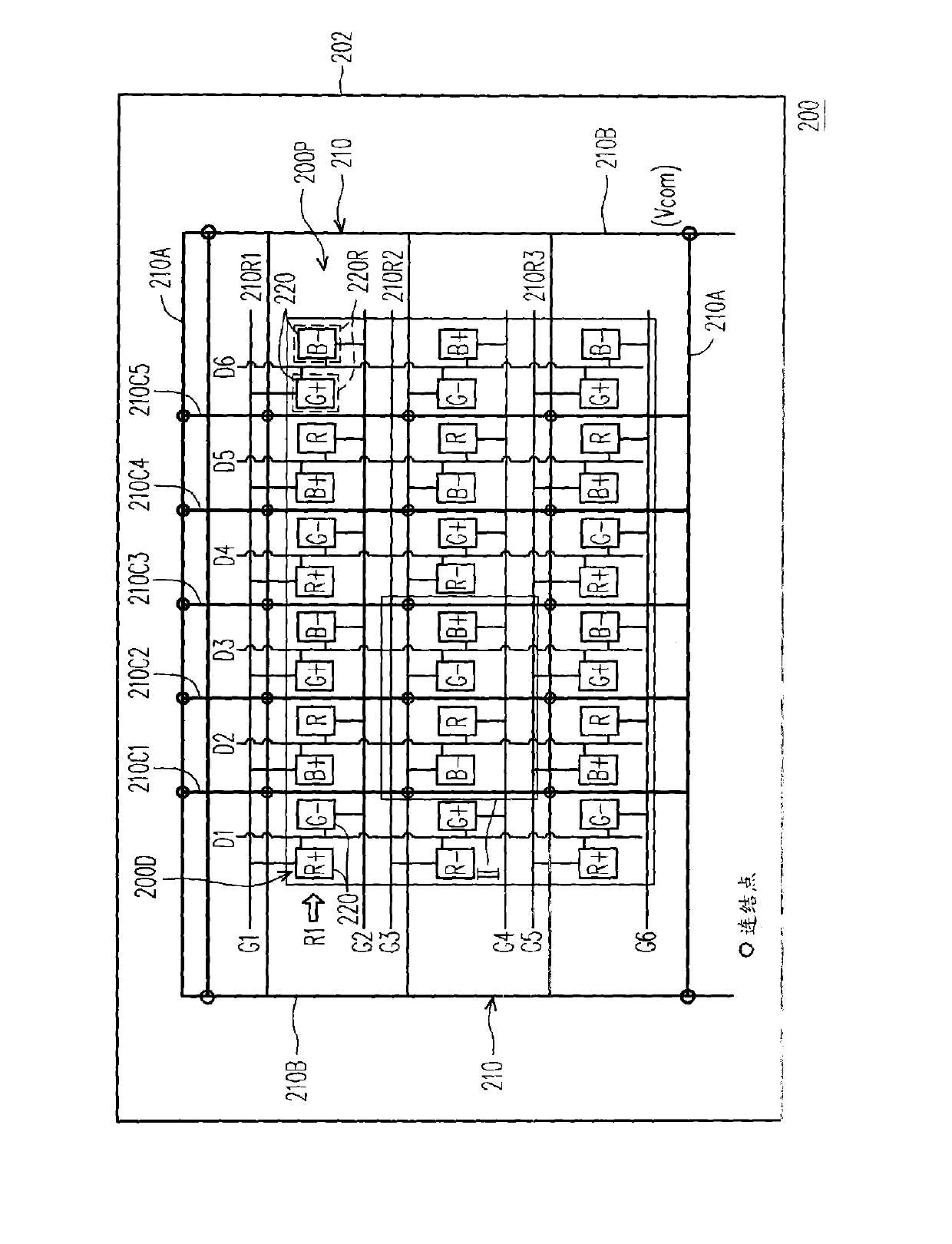
[0035] Figure 1A It is a top view of a dual scanning line pixel array substrate in an embodiment of the present invention. Please refer to Figure 1A , the dual scanning line pixel array substrate 200 has a display area 200D and a peripheral circuit area 200P outside the display area 200D, such as Figure 1A As shown, the dual scan line pixel array substrate 200 includes a plurality of scan lines G extending laterally, a plurality of data lines D extending vertically, a plurality of pixels 220 and a common wiring 210 . Specifically, the data line D intersects the scan line G, and two pixel regions 220R located on opposite sides of each data line D and adjacent to each other are defined in the display area 200D, and each pixel 220 is located in each within the pixel region 220R. It is worth noting that two adjacent scan lines G are electrically connected to a column of pixels 220 located therebetween, and the odd number of pixels 220 in the same column are connected to one of ...


PUM


Abstract

The invention provides a dual scanning line pixel array substrate, which comprises a substrate, a first conductive layer, a grid insulation layer, a semiconductor layer, a second conductive layer, a protective layer and a transparent electrode layer. The first conductive layer consists of a plurality of grids and a plurality of scanning lines. The grid insulation layer is covered on the first conductive layer. The semiconductor layer is arranged on the grid insulation layer; the semiconductor layer consists of a plurality of channel areas, a plurality of first common wires and a plurality of capacitance electrodes; and the first common wires are crossed with the scanning lines and connected with the capacitance electrodes. The second conductive layer is arranged on a part of the semiconductor layer and the grid insulation layer and consists of a plurality of sources, a plurality of drains and a plurality of data wires, wherein the first common wires are parallel to the data wires. The transparent electrode layer is electrically connected with each drain through each contact window of the protective layer; and the transparent electrode layer is overlapped with the protective layer and the capacitance electrodes of the semiconductor layer to form a storage capacitor.

Description

【Technical field】 [0001] The present invention relates to a display array substrate, and in particular to a dual scanning line pixel array substrate. 【Background technique】 [0002] With the development of large-sized display panels, among the pixel array structures of current liquid crystal display panels, there is a structure called half source driving (HSD for short). The HSD architecture can halve the number of data lines, so the price of the source driver will be relatively reduced. More specifically, in the pixel array of the HSD architecture, two adjacent sub-pixels share one data line, thereby reducing the number of data lines by half. [0003] Although the display panel adopting the HSD architecture can halve the number of driving channels of the source driver, since the odd and even pixels in the same column of pixels are connected to different scanning lines, the number of scanning lines in the HSD architecture is doubled. , so the pixel array substrate of the H...

Claims


Application Information

Patent Timeline
Patent Type & Authority Applications(China)
IPC IPC(8): G02F1/1362H01L27/02
Inventor 李俊谊周秀峰
Owner CENTURY DISPLAY (SHENZHEN) CO LTD
Why Eureka
Try Eureka