
Method for manufacturing P-type metal oxide semiconductor

An oxide semiconductor and metal technology, applied in semiconductor/solid-state device manufacturing, electrical components, circuits, etc., can solve the problems of low BVds of PMOS, PMOS damage, easy to be broken down, etc., to improve the source-drain breakdown voltage. Effect

Inactive Publication Date: 2011-09-14
FOUNDER MICROELECTRONICS INT
View PDF0 Cites 0 Cited by
  • Summary
  • Abstract
  • Description
  • Claims
  • Application Information

AI Technical Summary

Problems solved by technology

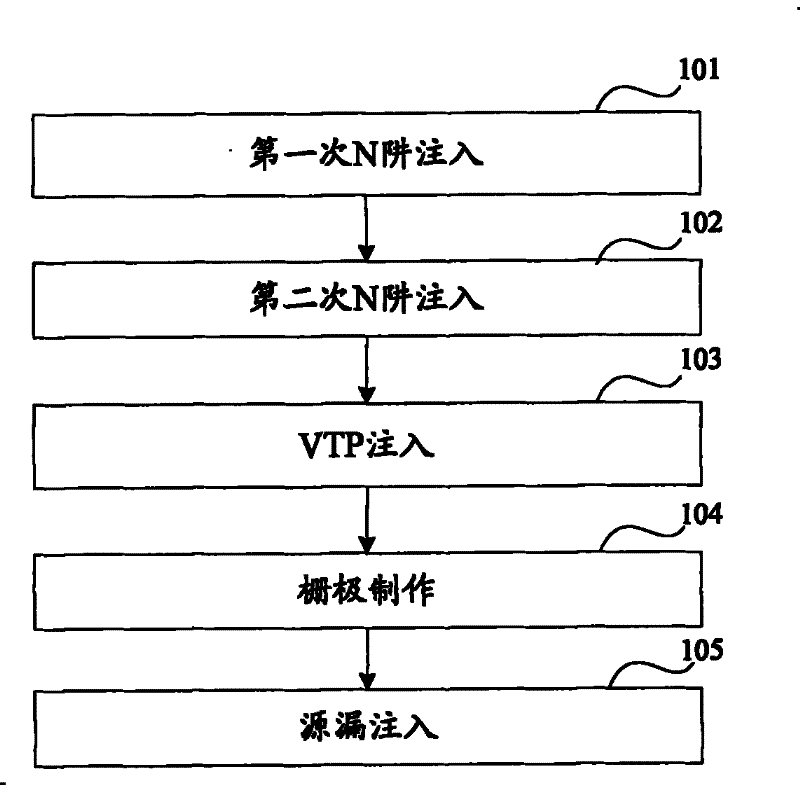
[0003] The level of BVds is related to the manufacturing process of PMOS. The traditional manufacturing process mainly includes four steps, namely, N-well injection, PMOS threshold voltage (VTP) injection, gate manufacturing, and source-drain injection. In the process of using the product, it is found that, The BVds of the PMOS obtained by the traditional manufacturing process is relatively low, and it is easy to be broken down during use, thereby causing damage to the PMOS. Therefore, how to improve the BVds of the PMOS is a common concern in the industry.

Method used


Image

  • Method for manufacturing P-type metal oxide semiconductor
  • Method for manufacturing P-type metal oxide semiconductor
  • Method for manufacturing P-type metal oxide semiconductor

Examples


Embodiment Construction

[0019] In order to improve the breakdown voltage of P-type metal oxide semiconductors, the embodiment of the present invention proposes a method for manufacturing P-type metal oxide semiconductors. The main realization principle, specific implementation process and its The corresponding beneficial effects that can be achieved are described in detail.

[0020] Before implementing the embodiment of the present invention, the traditional manufacturing process of PMOS was studied, and it was found that the process of well implantation has a key influence on the source-drain breakdown voltage BVds of PMOS, because the process of well implantation is directly related to the ion concentration on the surface of the PMOS channel Generally, the lower the ion concentration on the channel surface, the faster the carrier holes on the PMOS channel surface will decrease with the increase of the applied gate voltage Vg, and correspondingly, the faster the electrons will accumulate, so the chan...


PUM


Abstract

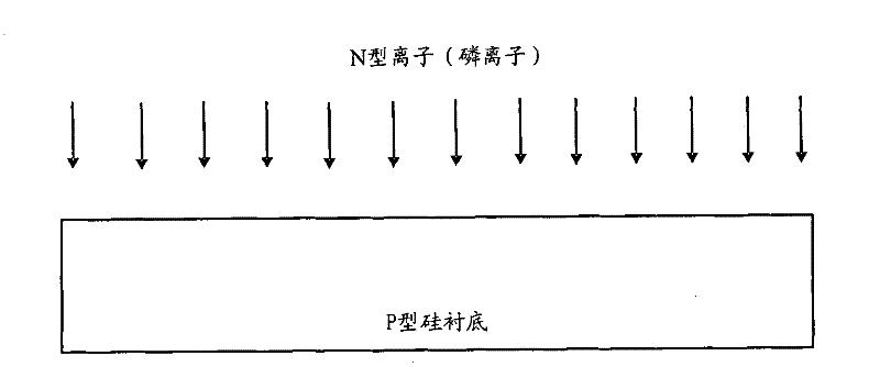
The invention discloses a method for manufacturing a P-type metal oxide semiconductor, comprising: carrying out phosphorous ion implantation and arsenic ion implantation on a silicon chip to form an N well; carrying out threshold voltage VTP implantation of P-type metal oxide semiconductor (PMOS) on the silicon chip with the N well; manufacturing grids for the silicon chip made by the VTP implantation; and carrying out source-drain implantation on the silicon chip made by the grids. By adopting the technical scheme provided by the embodiment, as the arsenic ions which are more than double of atomic weight of phosphorous ions in N-type ions are implanted twice during PMOS manufacture, the ion concentration on the surface of the silicon chip is much higher than that on the surface of PMOS produced by the traditional technology, thus greatly boosting source-drain breakdown voltage.

Description

technical field [0001] The invention belongs to the technical field of semiconductor chip manufacturing technology, and in particular relates to a method for manufacturing a P-type metal oxide semiconductor. Background technique [0002] The source-drain breakdown voltage (BVds) refers to the maximum drain-source voltage that the PMOS can withstand when the gate-source voltage Vgs is constant, that is, the limit operating voltage of the PMOS. Once the operating voltage exceeds BVds, it may cause damage to the PMOS. Therefore, BVds is a very important electrical parameter for the PMOS tube. The higher the BVds that the PMOS can achieve, the better the performance of the PMOS tube. [0003] The level of BVds is related to the PMOS manufacturing process. The traditional manufacturing process mainly includes four steps, namely, N-well injection, PMOS threshold voltage (VTP) injection, gate fabrication, and source-drain injection. During the use of the product, it was found that,...

Claims


Application Information

Patent Timeline
Patent Type & Authority Patents(China)
IPC IPC(8): H01L21/336H01L21/265
Inventor 李若加谭志辉黎智
Owner FOUNDER MICROELECTRONICS INT
Learn More