Manufacturing method of semiconductor memory

A manufacturing method, semiconductor technology, applied in the direction of semiconductor/solid-state device manufacturing, electrical components, circuits, etc., can solve the obstacles of miniaturization or high integration of semiconductor memory, affect device performance, and make it difficult to keep the grid structure of grid array 15 straight And other issues

Inactive Publication Date: 2010-07-14
SEMICON MFG INT (SHANGHAI) CORP
View PDF0 Cites 6 Cited by
  • Summary
  • Abstract
  • Description
  • Claims
  • Application Information

AI Technical Summary

Problems solved by technology

[0008] Firstly, the thicker the gate array 15 is, the more difficult it is to control its shape, that is, the more difficult it is to keep the straightness of each gate structure in the gate array 15 during the etching process, and it is easy to cause a short circuit between two adjacent word lines WL.
[0009] In addition, with the development of semiconductor integrated circuit technology, the integration level of semiconductor memory is increasing day by day, and the gap between gate arrays 15 is also getting smaller and smaller, but its thickness cannot be reduced accordingly because of the APT injection process, so , the resistance value of the unit length of each gate structure in the gate array 15 increases proportionally to the reciprocal of its width, which seriously affects the performance of the device and brings obstacles to the further miniaturization or high integration of semiconductor memories.

Method used


Image

  • Manufacturing method of semiconductor memory
  • Manufacturing method of semiconductor memory
  • Manufacturing method of semiconductor memory

Examples


Embodiment 1

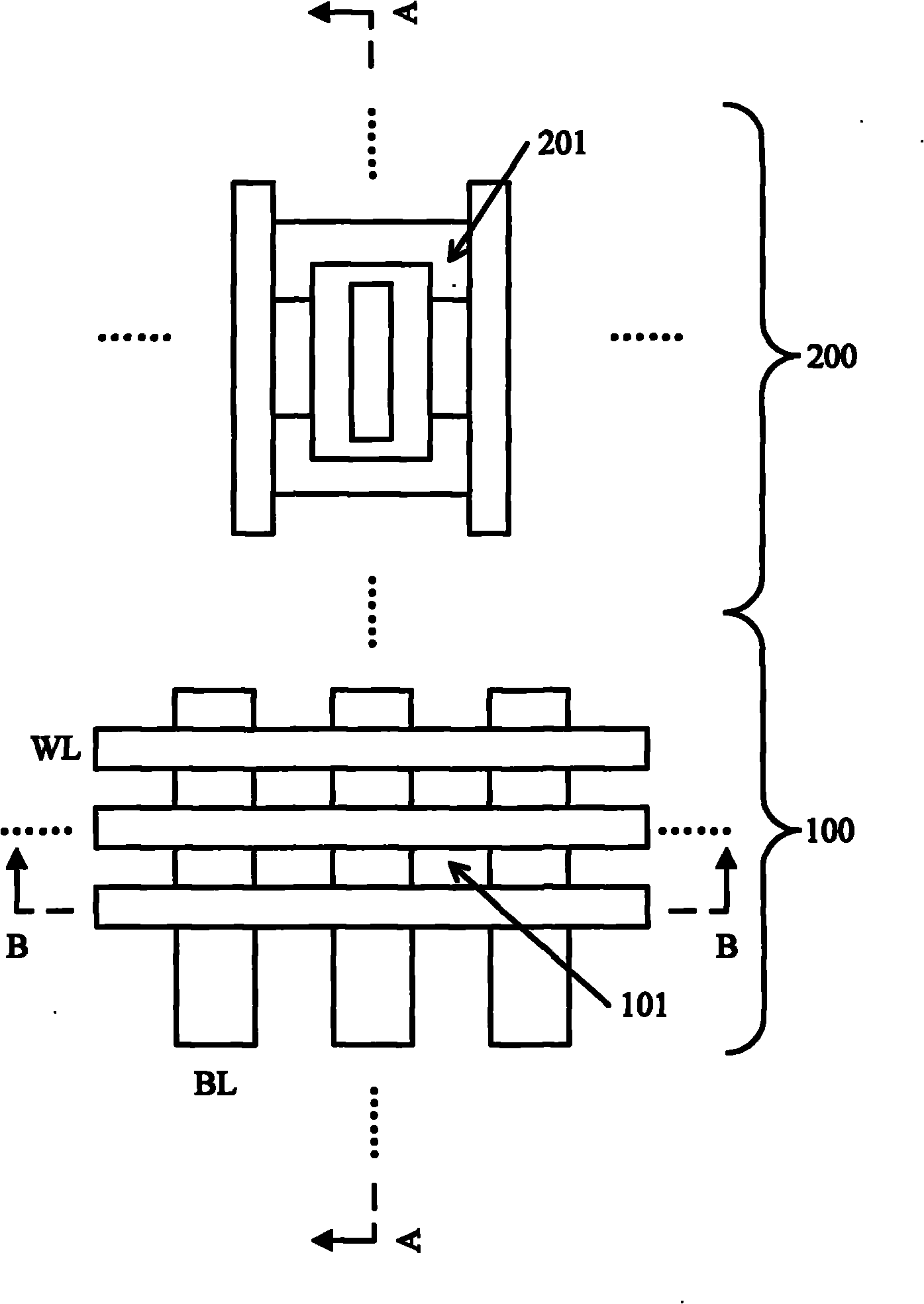
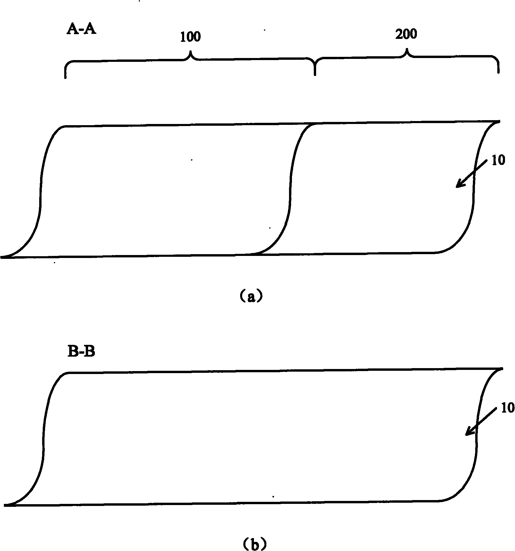
[0037] Please refer to Figure 9 , in the schematic diagram of the semiconductor memory manufacturing process given by it, the definition and etching of the gate array in the memory cell area come first, and the definition and etching of the gate of the logic transistor in the peripheral circuit area follow, as follows:

[0038] S11: providing a semiconductor substrate having a memory cell area and a peripheral circuit area;

[0039] S12: forming a gate material layer on the semiconductor substrate;

[0040] S13: forming a first mask on the gate material layer, the first mask covers the peripheral circuit area and defines a gate array in the memory cell area;

[0041] S14: using the first mask as a barrier layer, etching to form a gate array;

[0042] S15: Perform anti-penetration (APT) implantation using the first mask as a barrier layer;

[0043] S16: removing the first mask;

[0044] S17: forming a second mask on the gate material layer, the second mask covers the memor...

Embodiment 2

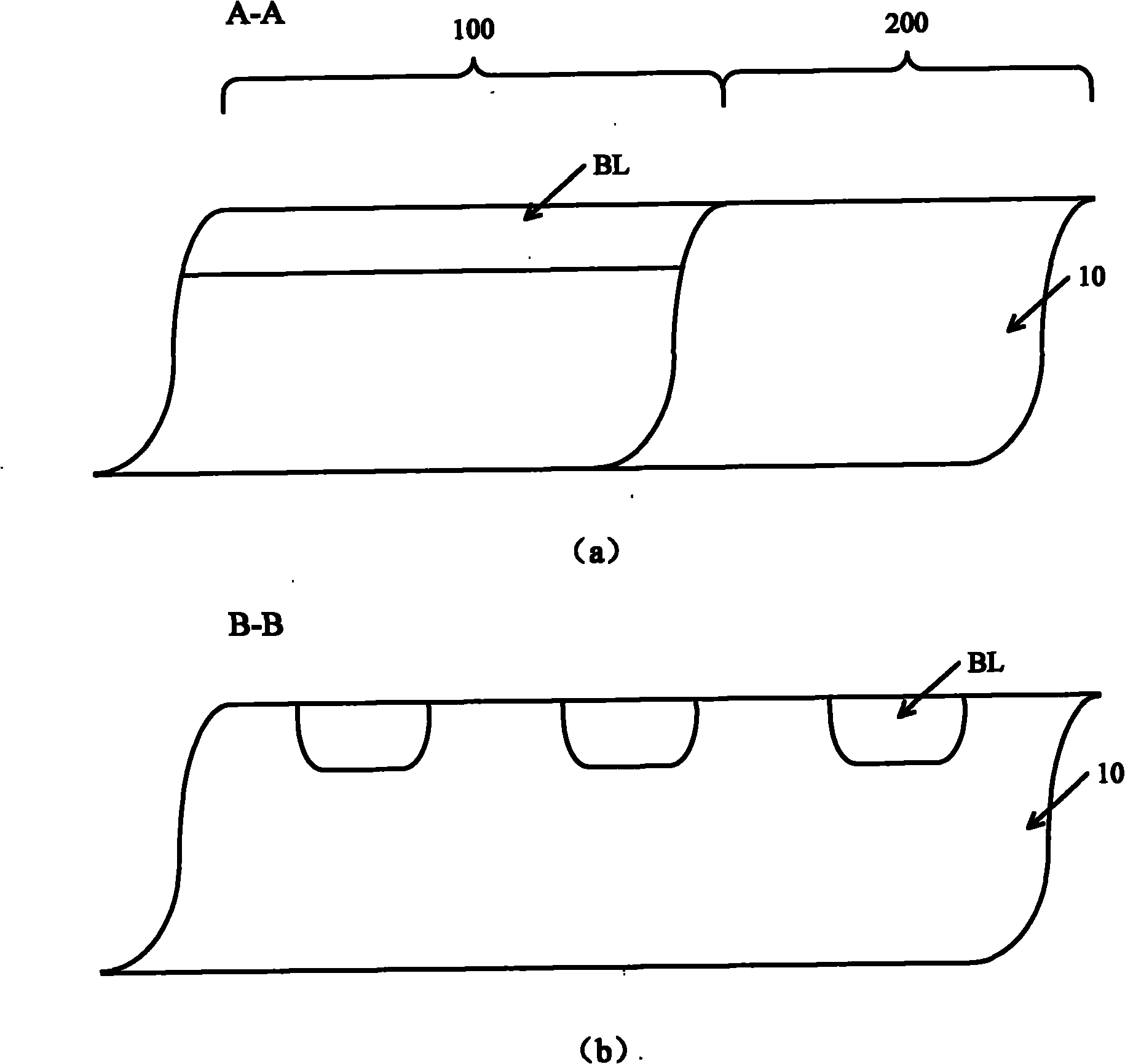
[0048] Please refer to Figure 10 , in the schematic diagram of the semiconductor memory manufacturing process given by it, the definition and etching of the gate of the logic transistor in the peripheral circuit area come first, and the definition and etching of the gate array in the memory cell area follow, as follows:

[0049] S21: providing a semiconductor substrate having a memory cell region and a peripheral circuit region;

[0050] S22: forming a gate material layer on the semiconductor substrate;

[0051] S23: forming a second mask on the gate material layer, the second mask covers the memory cell area and defines the gate of the logic transistor in the peripheral circuit area;

[0052] S24: Using the second mask as a barrier layer, etch to form the gate of the logic transistor;

[0053] S25: removing the second mask;

[0054] S26: forming a first mask on the gate material layer, the first mask covers the peripheral circuit area and defines a gate array in the memor...


PUM


Abstract

The invention discloses a manufacturing method of a semiconductor memory, comprising the following steps of: providing a semiconductor substrate with a memory unit zone and a peripheral circuit zone; forming a grid substance layer on the semiconductor substrate; forming a first masking film on the grid substance layer, wherein the first masking film shields the peripheral circuit zone and defines a grid allay in the memory unit zone; etching to form the grid allay by using the first masking film as a barrier layer; and carrying out anti-penetration (APT) injection by using the first masking film as the barrier layer. Therefore, different form the traditional method utilizing the grid allay as the barrier layer for the APT injection, the manufacturing method retains the masking film for defining the grid allay of the memory unit zone and uses the masking film as the barrier layer for the APT injection to reduce the association degree of the thickness of the grid allay and the APT injection, thereby reducing the thickness of the grid array according to other performance requirements of the memory unit zone, and then improving the integration level of the semiconductor memory.

Description

technical field [0001] The invention relates to the field of semiconductor manufacturing, in particular to a manufacturing method of a semiconductor memory. Background technique [0002] Semiconductor memory is a solid-state electronic device for storing data information made by semiconductor integrated circuit technology, which is composed of a large number of storage units and input and output circuits. Compared with magnetic memory, semiconductor memory has the advantages of fast access speed, large storage capacity, small size, etc., and the memory cell array is compatible with the main peripheral logic circuit, and can be manufactured on the same chip, which greatly simplifies the input and output interface. Therefore, semiconductor memory has been widely used in electronic products such as computers, and has become an important component of electronic products such as computers. [0003] figure 1 A schematic diagram of a partial planar structure of a semiconductor me...

Claims


Application Information

Patent Timeline
Patent Type & Authority Applications(China)
IPC IPC(8): H01L21/8234H01L21/027
Inventor 徐丹杨中辉刘经国孙士祯
Owner SEMICON MFG INT (SHANGHAI) CORP
Why Eureka
Try Eureka