Wafer level vacuum packaging method of MEMS (Micro-electromechanical System) component

A vacuum packaging, wafer-level technology, applied in decorative arts, microstructure devices, manufacturing microstructure devices, etc., can solve the problems of manufacturing process pollution, complex processing technology of MEMS devices, etc., to reduce pollution, improve process compatibility, The effect of improving performance

Active Publication Date: 2010-07-21
THE 13TH RES INST OF CHINA ELECTRONICS TECH GRP CORP
View PDF0 Cites 22 Cited by
  • Summary
  • Abstract
  • Description
  • Claims
  • Application Information

AI Technical Summary

Problems solved by technology

[0005] The technical problem to be solved by the present invention is to provide a wafer-level vacuum packaging method for ...

Method used


Image

  • Wafer level vacuum packaging method of MEMS (Micro-electromechanical System) component
  • Wafer level vacuum packaging method of MEMS (Micro-electromechanical System) component
  • Wafer level vacuum packaging method of MEMS (Micro-electromechanical System) component

Examples


Embodiment Construction

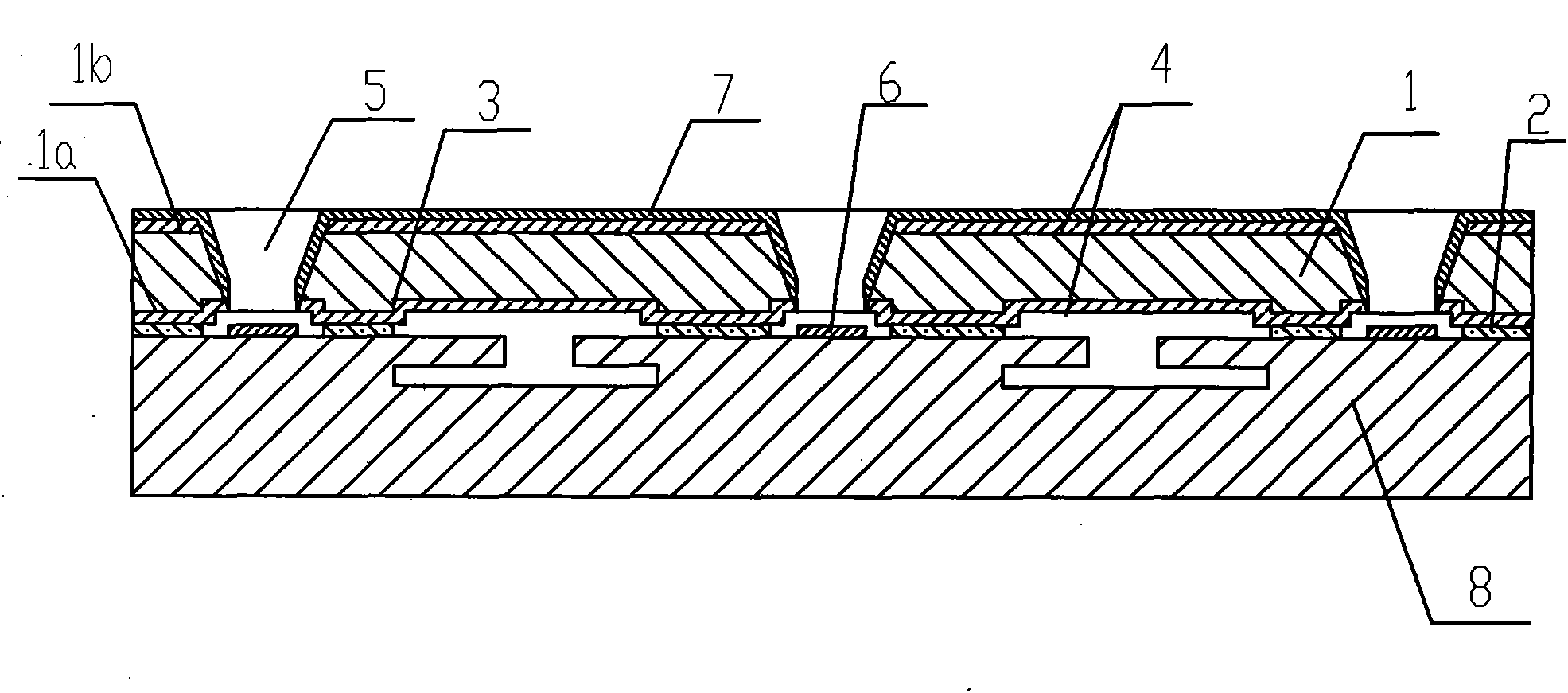
[0014] figure 1 It is a schematic diagram of the package structure of a MEMS device unit. From top to bottom, there are package cover plate 1 and MEMS device 8 in sequence. The package cover plate 1 and MEMS device 8 are bonded together by gold-silicon eutectic bonding.

[0015] Combine below Figure 2-1 to Figure 2-12 Specific embodiments of the present invention will be described.

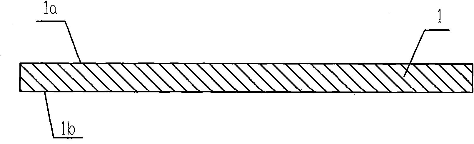
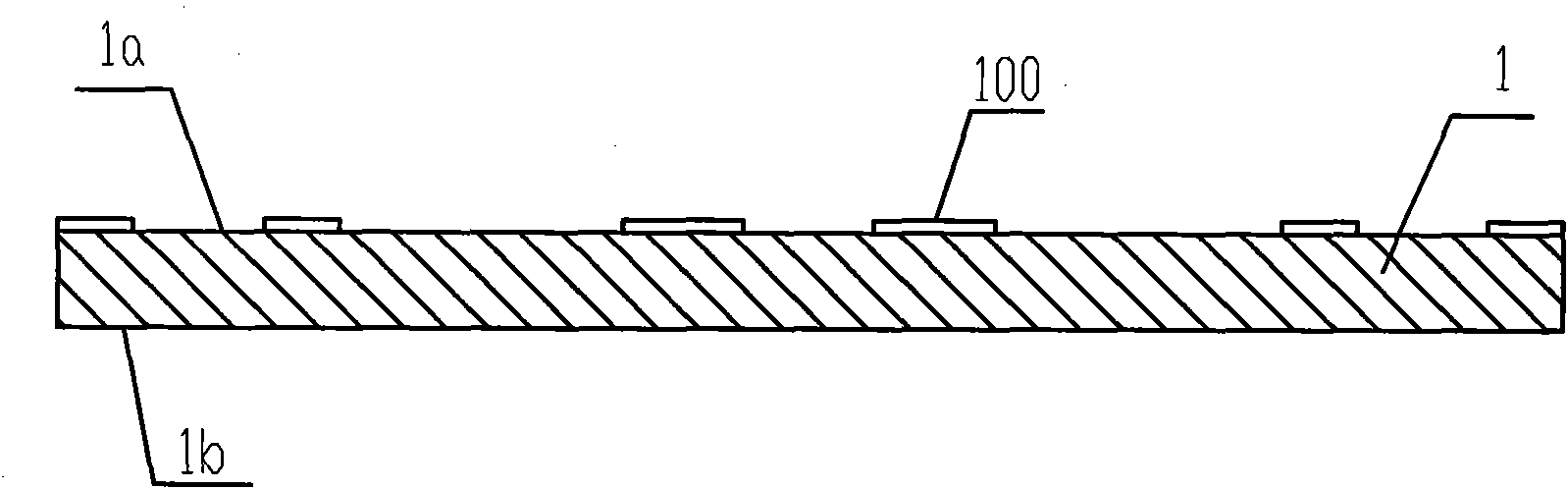
[0016] A MEMS device wafer-level vacuum packaging method, the steps of the method include: 1) depositing a metal film 2 for gold-silicon bonding on the MEMS device, 2) polishing the packaging cover plate 1 on both sides, 3) depositing the packaging cover plate 1 on both sides insulating dielectric 4, 4) etching the electrode lead-out via hole 5, 5) using gold-silicon eutectic bonding technology to bond and package the package cover plate 1 and MEMS device 8, 6) through deposition, photolithography, etching Prepare the lead-out electrode of the MEMS device on the surface of the MEMS device corre...


PUM


Abstract

The invention discloses a wafer level vacuum packaging method of an MEMS (Micro-electromechanical System) component, which realizes the packaging of a packaging cover plate and the MEMS component by adopting an eutectic bonding technology. The method comprises the steps of: (1) carrying out double-side polishing on the packaging cover plate; (2) depositing insulating media on two sides of the packaging cover plate; (3) preparing a metal film which is used for metal-silicon bonding on the packaging cover plate; (4) preparing an electrode outlet through hole; and (5) carrying out bonding packaging on the packaging cover plate and the MEMS component. By preparing the metal film which is used for metal-silicon bonding on the packaging cover plate, the invention omits the process for preparing bonding metal layer during processing the MEMS component, reduces the pollution of metal to MEMS components in production process, improves the process compatibility and further improves the performance of the MEMS components.

Description

technical field [0001] The invention relates to a packaging method, in particular to a wafer-level vacuum packaging method for MEMS (micro-electro-mechanical system) devices. Background technique [0002] MEMS packaging technology is an important research direction in the field of MEMS research. On the one hand, packaging can prevent MEMS products from being affected by dust, moisture, etc. on movable structures. On the other hand, vacuum or airtight packaging can also change the internal damping of MEMS products conditions and improve product performance. [0003] Wafer-level packaging technology is the main solution to achieve high performance, low cost and batch production of MEMS devices. Wafer-level packaging uses bonding technology to add a cover plate to the wafer of MEMS devices to complete the package, so it has the advantage of batching , and since expensive packaging shells can be omitted, packaging costs can be minimized. Bonding technologies for wafer-level pa...

Claims


Application Information

Patent Timeline
IPC IPC(8): B81C1/00
Inventor 徐永青杨拥军胥超罗蓉
Owner THE 13TH RES INST OF CHINA ELECTRONICS TECH GRP CORP
Why Eureka
Try Eureka