
High frequency switch circuit for inhibiting substrate bias effect in sampling hold circuit

A sample-and-hold circuit and high-frequency switching technology, which is applied in the direction of electrical components, output power conversion devices, etc., can solve the problems of affecting the accuracy of holding signals, the decline of circuit linearity, and the stability of thresholds, and achieve high-precision holding functions , good linearity, and the effect of improving the signal-to-noise-distortion ratio

Inactive Publication Date: 2010-07-21
ZHEJIANG UNIV
View PDF0 Cites 11 Cited by
  • Summary
  • Abstract
  • Description
  • Claims
  • Application Information

AI Technical Summary

Problems solved by technology

[0004] 1. When the frequency of the input signal is high, the CMOS transmission gate has a small signal charge feedthrough effect, which affects the accuracy of maintaining the signal, and is not allowed by the system in high-precision applications
[0005] 2. Since the substrate of the CMOS transmission gate is generally connected to the highest potential of the circuit (for PMOS transistors) or the closest potential (for NMOS transistors), the inconsistency between the substrate and source voltage leads to the substrate bias effect, which affects the stability of the threshold , which leads to a decrease in the linearity of the circuit
[0006] The existing technology cannot solve the above two problems at the same time, that is, under the high-frequency signal input, it can not only suppress the charge feedthrough effect but also suppress the threshold voltage change caused by the substrate bias effect.

Method used


Image

  • High frequency switch circuit for inhibiting substrate bias effect in sampling hold circuit
  • High frequency switch circuit for inhibiting substrate bias effect in sampling hold circuit
  • High frequency switch circuit for inhibiting substrate bias effect in sampling hold circuit

Examples


Embodiment Construction

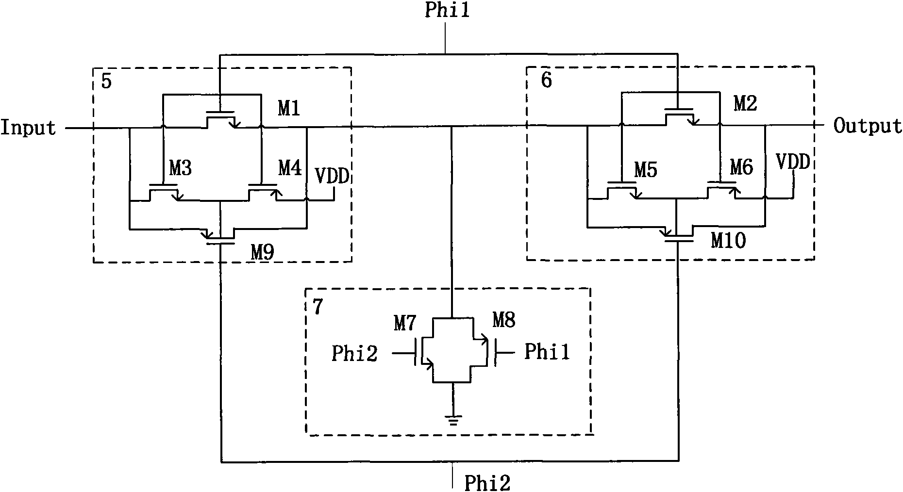
[0034] Such as figure 2 As shown, the high-frequency switch circuit for suppressing the substrate bias effect in the sample-and-hold circuit of the present invention includes three parts: the first substrate bias suppression high-frequency switch unit 5, the second substrate bias suppression high-frequency switch unit 6 and transmission gate switch 7.

[0035] One end of the first substrate bias suppression high-frequency switch unit 5 is connected to the input signal terminal Input, and the other end is connected to the second substrate bias suppression high-frequency switch unit 6 and the transmission gate switch 7; the second substrate bias suppression is high One end of the frequency switch unit 6 is connected to the first substrate bias suppression high frequency switch unit 5 and the transmission gate switch 7, and the other end is connected to the output signal terminal Output.

[0036] The first suppression substrate bias high-frequency switch unit 5 includes:

[00...


PUM


Abstract

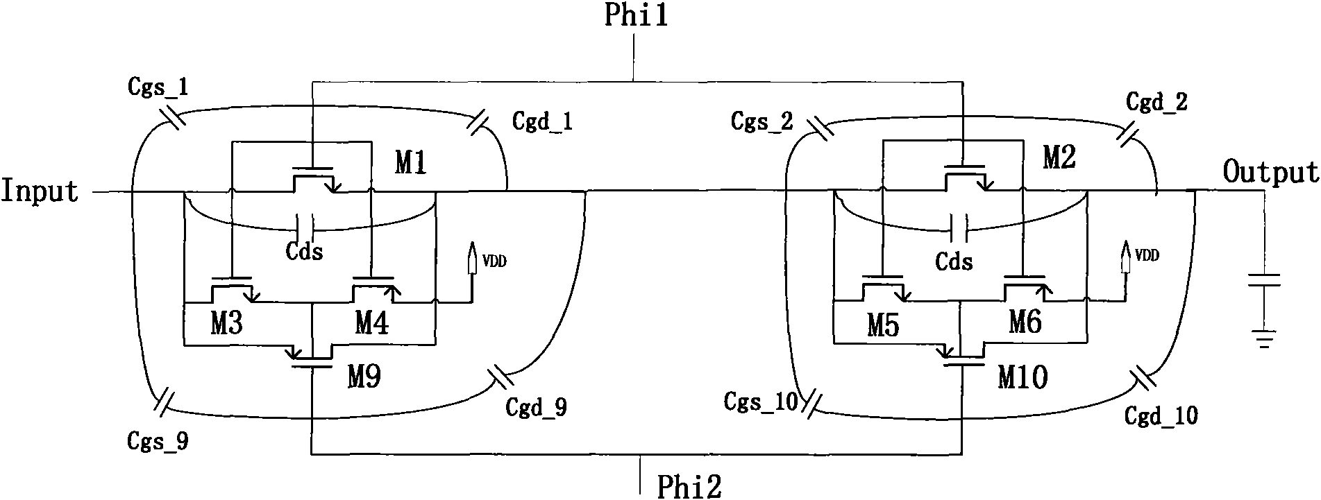
The invention discloses a high frequency switch circuit for inhibiting substrate bias effect in a sampling hold circuit, comprising a first substrate bias-inhibiting high frequency switch unit, a second substrate bias-inhibiting high frequency switch unit and a transmission gate switch, wherein the first substrate bias-inhibiting high frequency switch unit consists of two NMOS (N-channel Metal Oxide Semiconductor) transistors and two PMOS (P-channel Metal Oxide Semiconductor) transistors, the second substrate bias-inhibiting high frequency switch unit consists of two NMOS transistors and two PMOS transistors and the transmission gate switch consists of one NMOS transistor and one PMOS transistor. In the high frequency switch circuit, because a feed through signal introduced by a switch parasitic capacitor can be grounded through a by-pass, the variation of the input end does not affect the output end after the switch is turned off, thereby the hold function of high precision is realized. The switch design of inhibiting the substrate bias effect is utilized. Because the variation of a threshold voltage caused by the inequality of a substrate and a source electric potential is inhibited, the linearity of the equivalent resistance of the switch circuit is better and the signal-to-noise distortion ratio of the circuit is improved.

Description

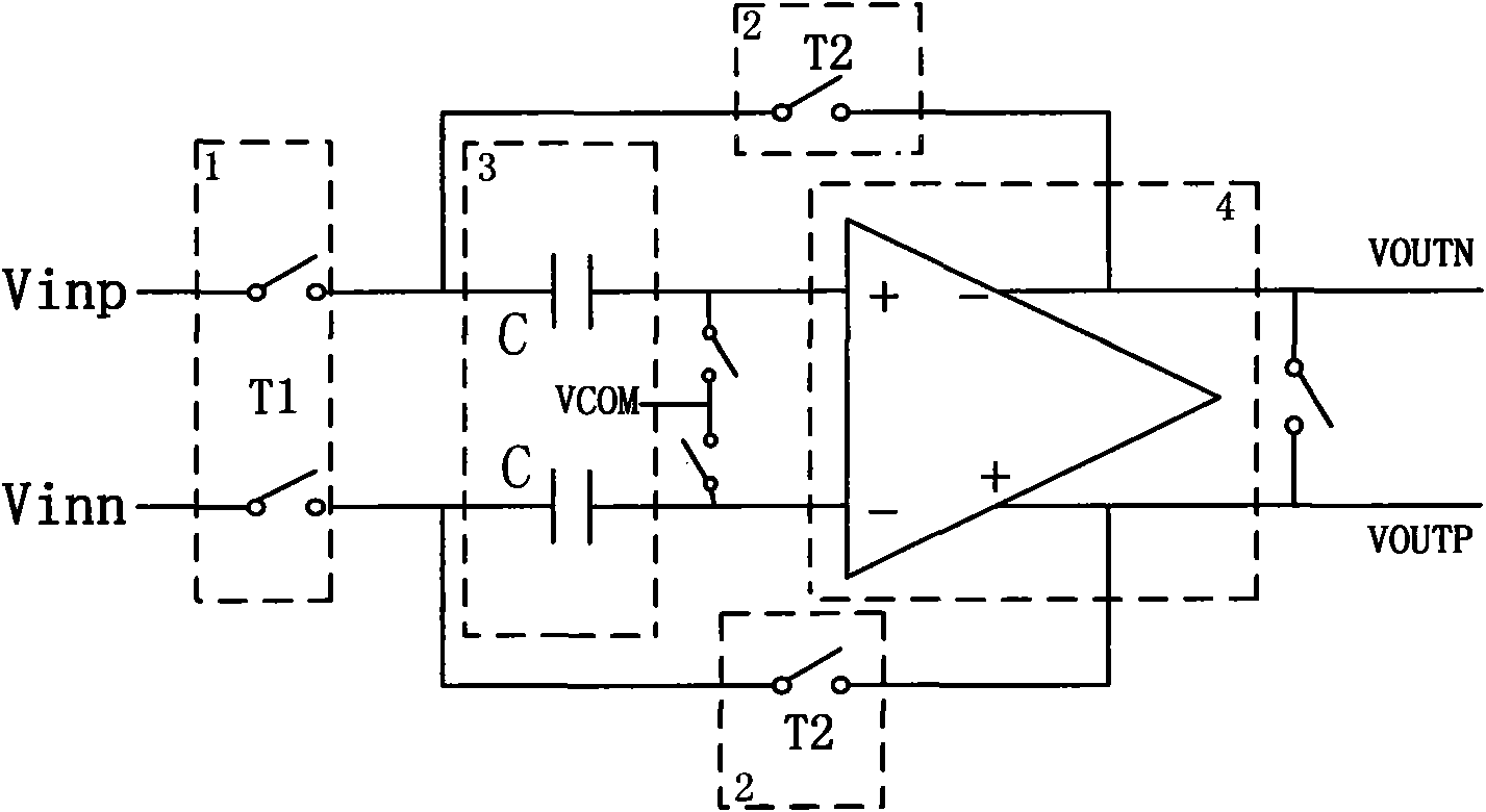
technical field [0001] The invention relates to a high-frequency switch circuit for suppressing substrate bias effect, which belongs to the technical field of integrated circuits. Background technique [0002] Now the module that is often used in the design of analog integrated circuits, its function is to complete the acquisition of analog input signals and keep them at the output for a certain period of time to facilitate the processing of subsequent signal processing circuits. Such as figure 1 The capacitor flipping switched capacitor sampling and holding circuit shown mainly includes an input sampling switch T1, an output holding switch T2, a sampling capacitor C, and an operational amplifier. When the sampling phase is valid, the sampling switch T1 is closed, the holding switch T2 is open, and the analog signal is collected on the sampling capacitor C; when the holding phase is valid, the sampling switch T1 is open, the holding switch T2 is closed, and the signal on th...

Claims


Application Information

Patent Timeline
Patent Type & Authority Applications(China)
IPC IPC(8): H02M1/08
Inventor 蔡坤明丁扣宝韩雁何杞鑫
Owner ZHEJIANG UNIV
Learn More