Spiral coil structure of lamination chip component inner electrode

A technology of components and inner electrodes, applied in the field of spiral coil structure, can solve the problems of reducing DC resistance, inductance or impedance, and achieve the effects of stress elimination, weak diffusion, and small magnetic leakage

Inactive Publication Date: 2010-07-28
SHENZHEN SUNLORD ELECTRONICS
View PDF5 Cites 9 Cited by
  • Summary
  • Abstract
  • Description
  • Claims
  • Application Information

AI Technical Summary

Problems solved by technology

However, due to the serious magnetic flux leakage between the parallel coils, the inductance or impedance is greatly reduced compared with the conventional non-parallel structure. Under the same inductance or impedance, this structure can only reduce the DC resistance to a limited extent.

Method used


Image

  • Spiral coil structure of lamination chip component inner electrode
  • Spiral coil structure of lamination chip component inner electrode
  • Spiral coil structure of lamination chip component inner electrode

Examples


specific Embodiment approach 1

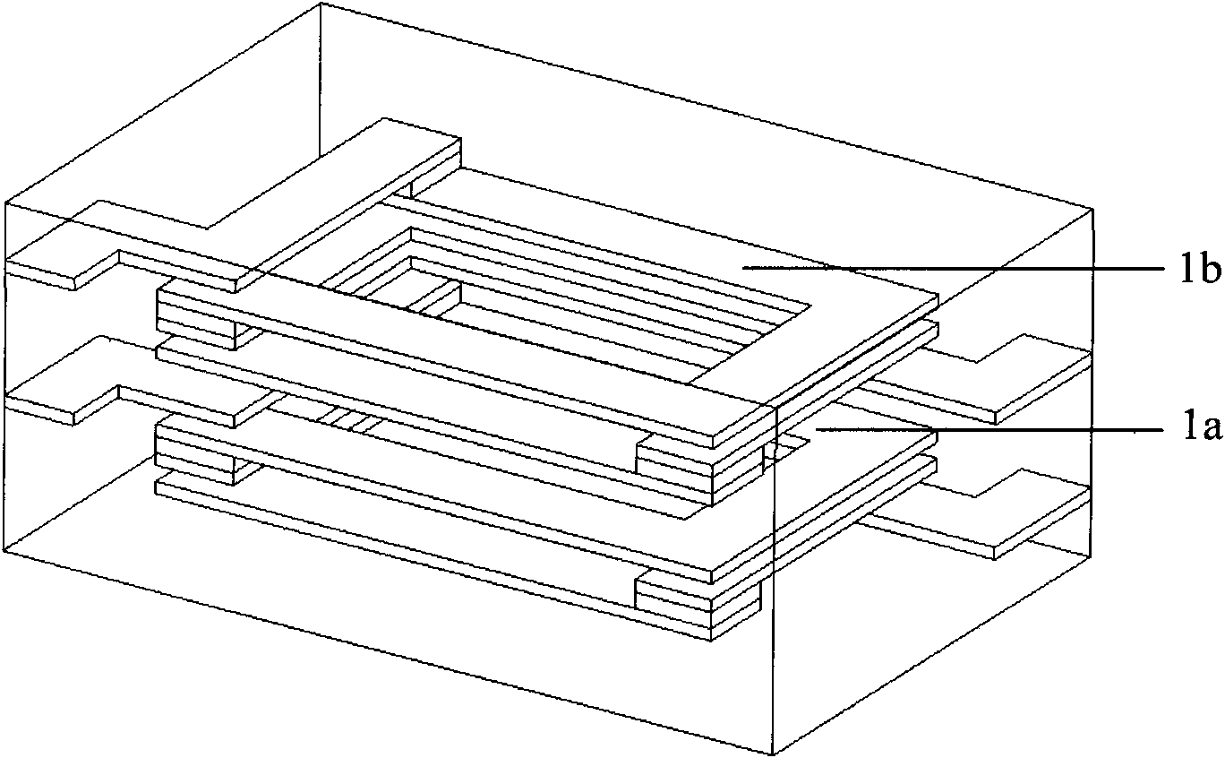
[0021] like figure 2 In the structure of the helical coil of the inner electrode of the laminated chip component shown, the helical coil 2 is divided into four sections by an upper lead-out 3 , a lower lead-out 4 and two electrodes 5 . The upper terminal 3, the lower terminal 4 and the two electrodes 5 are all connected in parallel by two electrodes of the same shape, and the DC resistance of each segment is reduced to 1 / 2 of each segment in the non-parallel state, so the total DC resistance of the helical coil The resistance is reduced to 1 / 2 of the non-parallel state. The upper lead-out 3 , the lower lead-out 4 and the parallel electrodes of the two electrodes 5 are completely or incompletely separated by electrically insulating thin-layer magnets (not shown in the figure). Both ends of the two coil-shaped electrodes 5 are connected by a conductive point 6, and one end of the upper lead-out terminal 3 and the lower lead-out end 4 is connected by the conductive point 6, and...

specific Embodiment approach 2

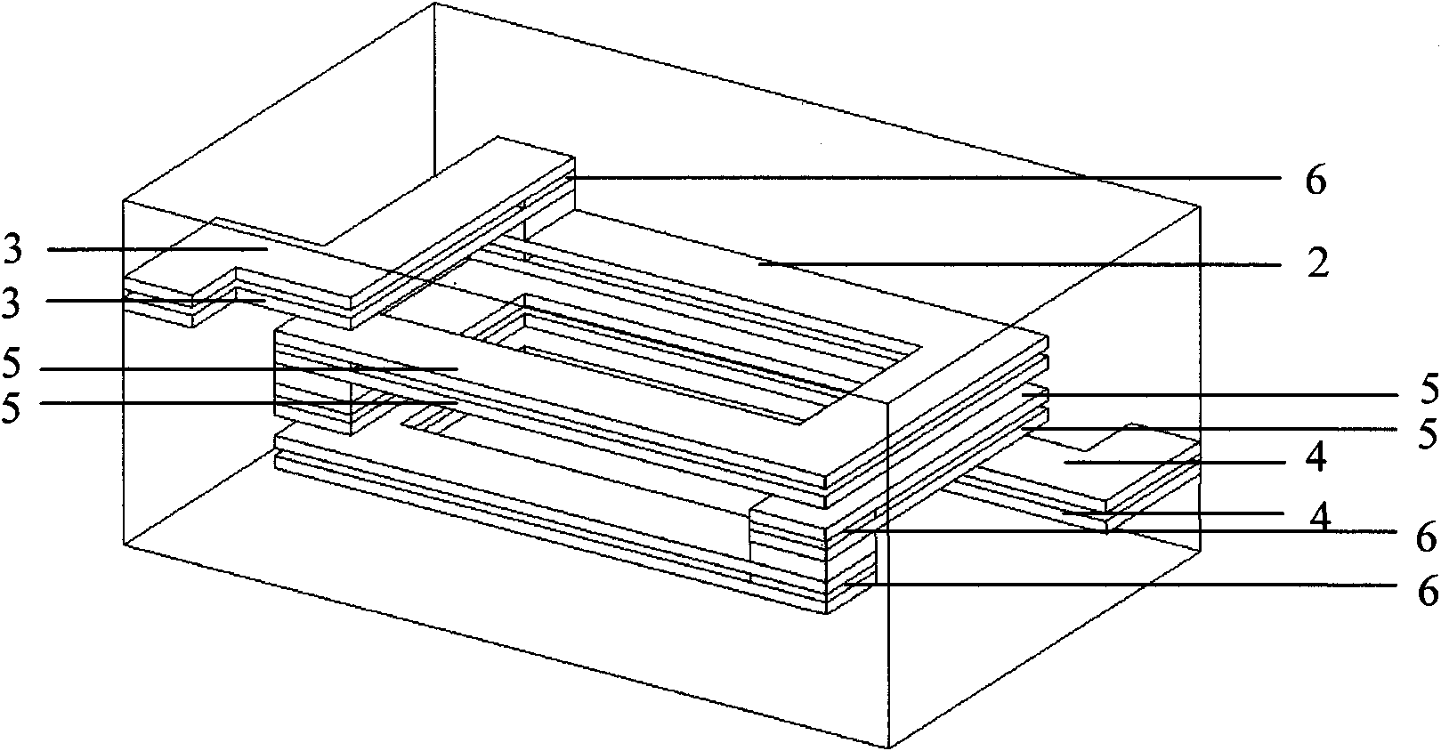
[0022] like image 3 In the structure of the helical coil of the inner electrode of the laminated chip component shown, the helical coil 2 is divided into four sections by an upper lead-out 3 , a lower lead-out 4 and two electrodes 5 . The lower terminal 4 and an electrode 5 are connected in parallel by two strands of electrodes with the same shape, and the DC resistance of the parallel segment is 1 / 2 of that of each segment in the non-parallel state, so the total DC resistance of the helical coil is greatly reduced. The parallel lower leads 4 and the parallel electrodes 5 are completely or partially separated by electrically insulating thin-layer magnets (not shown in the figure). Two ends of the parallel electrode 5 are connected by a conductive point 6, and one end of the parallel lower lead-out terminal 4 is connected by the conductive point 6, and the other end is connected by a common external terminal electrode (not shown in the figure). It can make the laminated chip ...

specific Embodiment approach 3

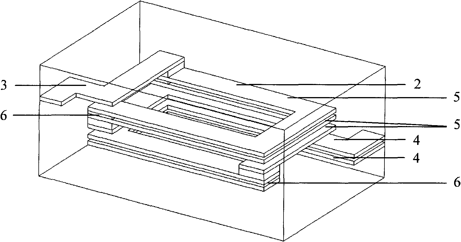
[0023] like Figure 4 In the shown structure of the helical coil of the internal electrode of the laminated chip component, the helical coil 2 is divided into two sections by the upper lead-out end 3 and the lower lead-out end 4 . The upper terminal 3 and the lower terminal 4 are connected in parallel by three terminal electrodes with the same shape, so the total DC resistance of the helical coil is reduced to 1 / 3 of that of the non-parallel state. One end of the upper lead-out terminal 3 and the lower lead-out end 4 is connected by a conductive point 6, and the other end is connected by a common external terminal electrode (not shown in the figure). It can make the laminated chip components maintain high inductance or impedance while greatly reducing the DC resistance, and will not cause short circuit of the laminated chip components and magnet cracking.


PUM


Abstract

The invention discloses a spiral coil structure of lamination chip component inner electrode. The spiral coil is formed by connecting at least two coil units; wherein the spiral coil is single solenoid coil, magnetic line of force is bound in the solenoid coil, the coil unit is formed by connecting at least two stranded electrodes which are in parallel connection from top to bottom and in the same shape, and at least two stranded electrodes are separated by electrically isolated thin magnet, and the two ends of at least two stranded electrodes are respectively connected. The direct current resistance of the spiral coil of the invention can be reduced to 1/2 or 1/N of the existing non-parallel structure, N is number of the stranded electrodes in parallel connection, and the spiral coil is single solenoid coil, magnetic line of force is bound in the solenoid coil, thus magnetic leakage is less, and inductance or impedance reduction amplitude of the spiral coil is less. Stress between electrode and magnet after sintering can be effectively eliminated, not only component magnet cracking is avoided but also diffusion is weaker and short circuit can not be caused.

Description

technical field [0001] The invention relates to a helical coil of an internal electrode, in particular to a structure of a helical coil of an internal electrode of a laminated chip component with large impedance and low DC resistance. Background technique [0002] In the case of the same external magnet, the more the number of spiral coils and the larger the coil area of ​​the inner electrode of the laminated chip component, the greater the inductance or impedance of the laminated chip component, and the energy storage or filtering The better the effect. However, when the number of coils of the helical coil of the inner electrode increases and the area of ​​the coil increases, the DC resistance of the helical coil also increases correspondingly, and the power loss when the current is passed is correspondingly greater. Therefore, it is necessary to reduce the DC resistance of the helical coil accordingly. [0003] There are three main ways to reduce the DC resistance at pre...

Claims


Application Information

Patent Timeline
Patent Type & Authority Applications(China)
IPC IPC(8): H01F27/28H01F17/04
Inventor 张扬郭海戴春雷
Owner SHENZHEN SUNLORD ELECTRONICS
Why Eureka
Try Eureka