Waveguide grating coupler with distributed Bragg reflector and manufacturing method thereof

A technology of Bragg reflector and waveguide grating, which is applied in the coupling of optical waveguide and other directions, can solve the problems of complex process and low coupling efficiency

Inactive Publication Date: 2010-08-04
INST OF SEMICONDUCTORS - CHINESE ACAD OF SCI
View PDF0 Cites 28 Cited by
  • Summary
  • Abstract
  • Description
  • Claims
  • Application Information

AI Technical Summary

Problems solved by technology

However, the grating coupler also faces the problem of low coupling efficiency. Although the coupling efficiency can be i...

Method used


Image

  • Waveguide grating coupler with distributed Bragg reflector and manufacturing method thereof
  • Waveguide grating coupler with distributed Bragg reflector and manufacturing method thereof
  • Waveguide grating coupler with distributed Bragg reflector and manufacturing method thereof

Examples


Embodiment Construction

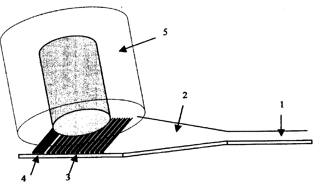
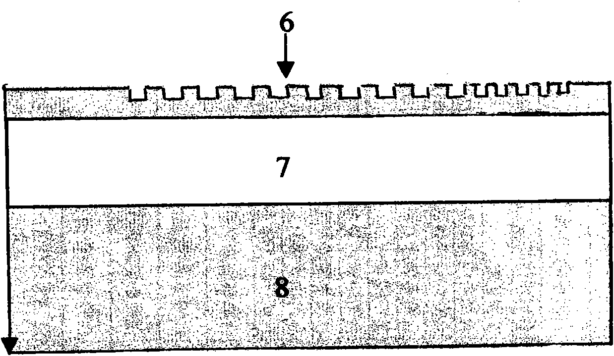
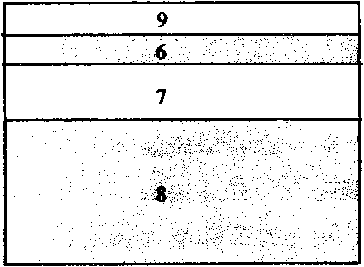
[0035] see figure 1 and figure 2 Shown, the present invention provides a kind of waveguide grating coupler with distributed Bragg reflector, and described coupler adopts the silicon material on the insulator, comprises:

[0036] A silicon substrate 8;

[0037] A confinement layer 7, the confinement layer 7 is made on the silicon substrate 8, the thickness of the confinement layer 7 is greater than 500nm, which can effectively prevent light from leaking to the silicon substrate 8;

[0038] A top silicon layer 6, the top silicon layer 6 is made on the confinement layer 7, a diffraction grating 3 is made on the surface of the top silicon layer 6, a reflection grating 4 is made on one side of the diffraction grating 3, and a reflection grating 4 is made on the side of the diffraction grating 3 The other side is a tapered waveguide 2, the tapered waveguide 2 is larger than 80 μm, which can realize lossless transmission in theory, and the connection with the tapered waveguide 2 i...


PUM

PropertyMeasurementUnit
Lengthaaaaaaaaaa
Thicknessaaaaaaaaaa
Thicknessaaaaaaaaaa

Abstract

The invention relates to a waveguide grating coupler with a distributed Bragg reflector. The coupler is made of silicon materials on an insulator and comprises a silicon substrate, a limiting layer, a top silicon layer and an optical fiber, wherein the limiting layer is made on the silicon substrate; the top silicon layer is made on the limiting layer; a diffraction grating is made on the surface of the top silicon layer; a reflection grating is made at one side of the diffraction grating; the other side of the diffraction grating is provided with a tapered waveguide with the length of about 80 micrometers; a submicrometer waveguide is arranged on the connecting point of the diffraction grating and the tapered waveguide; and one end of the optical fiber is close to the diffraction grating on the top silicon layer.

Description

technical field [0001] The invention relates to the technical field of photonic devices, and is a grating waveguide coupler. The structure of the grating coupler can effectively reduce the coupling loss of optical fibers and waveguides, and is easy to integrate. It is widely used in optical communication, chip optical interconnection and high-speed silicon-based optical integration. middle. Background technique [0002] Since the 1960s, optoelectronic integration (OEIC) has achieved considerable development. The mainstream trend of integrated circuit development is the miniaturization of integrated systems. Among the many waveguide materials used in the communication band, SOI material has become one of the most competitive materials for optical integration and electronic integration due to its unparalleled cost advantages, process maturity, and compatibility with IC processes. However, although SOI submicron waveguides can achieve many compact structures and excellent fun...

Claims


Application Information

Patent Timeline
IPC IPC(8): G02B6/34
Inventor 朱宇李智勇俞育德余金中
Owner INST OF SEMICONDUCTORS - CHINESE ACAD OF SCI
Why Eureka
Try Eureka