Light emitting diode device and packaging method therefore

A technology of light-emitting diodes and packaging methods, which is applied in the direction of electrical components, circuits, semiconductor devices, etc., and can solve problems such as increased manufacturing costs, increased manufacturing complexity of LED light-emitting devices, and increased volume of LED light-emitting devices, and achieves the effect of simplifying the manufacturing process

Inactive Publication Date: 2010-08-11
EVERLIGHT ELECTRONICS
View PDF0 Cites 37 Cited by
  • Summary
  • Abstract
  • Description
  • Claims
  • Application Information

AI Technical Summary

Problems solved by technology

However, in this way, in addition to the inevitable increase in the volume of the LED lighting device, the complexity of manufacturing the LED li

Method used


Image

  • Light emitting diode device and packaging method therefore
  • Light emitting diode device and packaging method therefore
  • Light emitting diode device and packaging method therefore

Examples


Example Embodiment

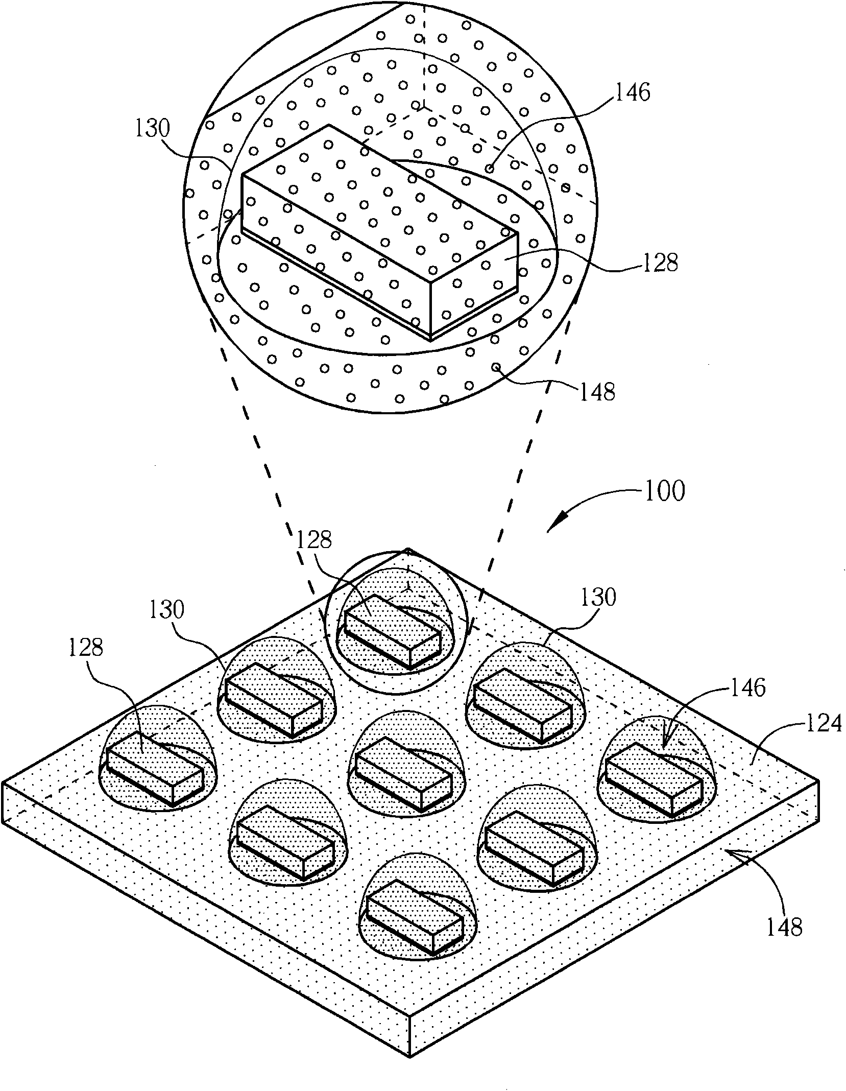
[0028] Please refer to Figure 1 to Figure 3 . figure 1 Is a schematic diagram of the structure of the LED device 100 according to the first preferred embodiment of the present invention, figure 2 for figure 1 A schematic top view of the first transparent substrate 124 shown, and image 3 for figure 1 The illustrated three-dimensional exploded schematic view of the LED chip 128 and the first transparent substrate 124 is shown. Such as figure 1 As shown, the LED device 100 may include a first transparent substrate 124, a plurality of LED chips 128 fixed on the first transparent substrate 124, and a transparent glue 130 covering the LED chips 128. Wherein, the first transparent substrate 124 may include any light-permeable material, such as a glass substrate or a plastic substrate. The LED chip 128 can be various types of LED chips. In a preferred case, the upper and lower surfaces of each LED chip 128 used can emit light uniformly. For example, the wavelength range of the emitte...


PUM


Abstract

The invention provides a light emitting diode device which comprises a transparent base plate, a plurality of light emitting diode chips, a circuit and a transparent colloid, wherein the light emitting diode chips are fixedly connected to the transparent base plate; the circuit is formed on the transparent base plate and is electrically connected to the light emitting diode chips; and the transparent colloid is used for packaging the light emitting diode chips. The light emitting diode chips are used for generating light rays with at least one type of wavelength, and the light generated by the light emitting diode chips is respectively emitted to two opposite surfaces of the transparent base plate. The blue light chips are welded on the circuit of the transparent base plate, the fluorescence material is matched and coated, and the advantages of the base plate are utilized, therefore the double-surface white light emitting device packaged by the chips is manufactured.

Description

technical field [0001] The present invention relates to a light emitting diode (light emitting diode, LED) device and its packaging method, especially to a light emitting diode device that can be used as a double-sided white light emitting device and its packaging method. Background technique [0002] Compared with traditional light sources such as cold cathode tubes, LED packaging components have small size, low power consumption, high brightness, high color performance, fast response (can be operated at high frequency), environmental protection (shock resistance, impact resistance and not easy to break) , recyclable) and easy to develop into light, thin and short products and other advantages, so LED light source has a certain market advantage. Generally speaking, a traditional LED packaging assembly basically includes a packaging cup and an LED chip mounted on the packaging cup. The traditional packaging cup holder has two internal connection terminals and two external c...

Claims


Application Information

Patent Timeline
IPC IPC(8): H01L33/00
Inventor 刘宇桓
Owner EVERLIGHT ELECTRONICS
Why Eureka
Try Eureka