Method for on-line detection of form of silicon nanocrystals

A silicon nanocrystal and nanocrystal technology, applied in the field of nanocrystal particle detection, can solve the problems of difficulty in quickly calculating the average value, unsuitable for rapid detection, long cycle, etc., and achieves the effects of convenient measurement, simple form and fast speed.

Active Publication Date: 2010-08-25
INST OF MICROELECTRONICS CHINESE ACAD OF SCI
View PDF0 Cites 8 Cited by
  • Summary
  • Abstract
  • Description
  • Claims
  • Application Information

AI Technical Summary

Problems solved by technology

[0005] However, both of these methods require fragment analysis, which has a long period and high cost. Moreover, these two methods mainly focus on detecting the shape o...

Method used


Image

  • Method for on-line detection of form of silicon nanocrystals
  • Method for on-line detection of form of silicon nanocrystals
  • Method for on-line detection of form of silicon nanocrystals

Examples


Embodiment Construction

[0031] In order to make the object, technical solution and advantages of the present invention clearer, the present invention will be described in further detail below in conjunction with specific embodiments and with reference to the accompanying drawings.

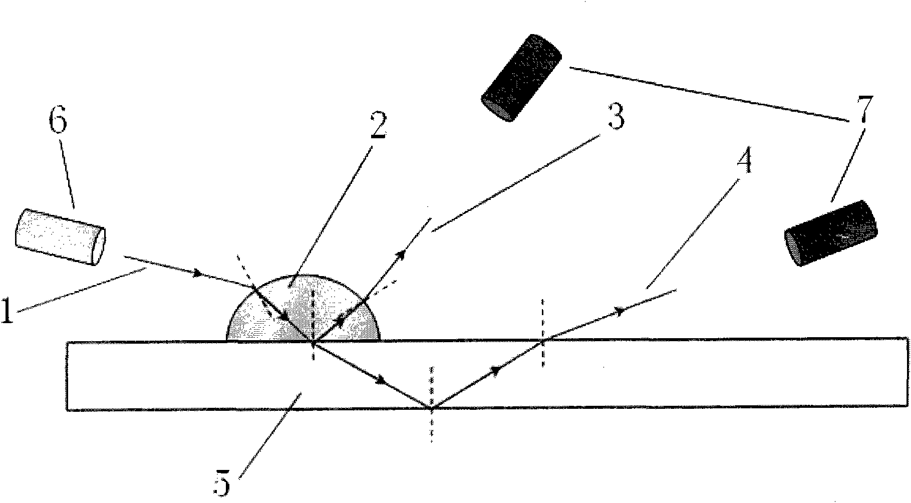
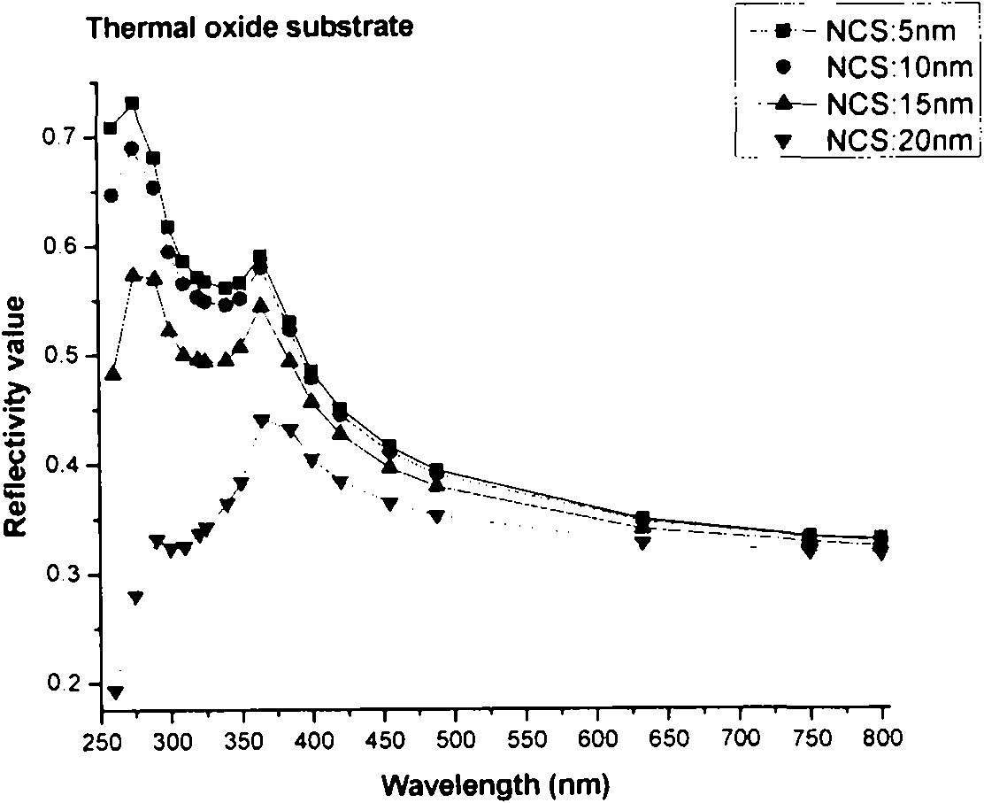
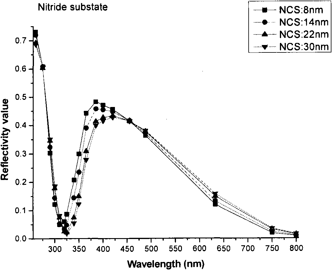
[0032] The method provided by the present invention for on-line detection of silicon nanocrystal morphology by measuring the change of reflectance of monochromatic light affects the change of reflected light intensity through the absorption of incident light by nanocrystal particles, resulting in regular changes in reflectivity. The nanocrystal morphology can be qualitatively linked to the reflectance of light, which enables the rapid online detection of silicon nanocrystals.

[0033] Such as figure 1 Shown, the realization principle of the present invention is as follows: for silicon dioxide (as diagram 2-1 ), the greater the density of nanocrystals, the greater the thickness, the greater the loss of incident light, an...


PUM


Abstract

The invention discloses a method for on-line detection of the form of silicon nanocrystals. The method comprises the following steps of: preparing a plurality of silicon plates serving as substrates, and growing a tunneling medium layer on the surface of each substrate; treating the surfaces of the substrates by using diluted hydrofluoric acid, and growing a layer of silicon nanocrystals on the surface of each substrate; irradiating incident light which is monochromatic light with a 365nm wave length onto the surfaces of the substrates, wherein because surface materials and shapes are different, the intensity of reflected light is certainly changed; recording reflection indexes of nanocrystalline silicon chips in various growth periods, and establishing an expression of the relationship between the growth periods and the reflection indexes; performing fragment analysis of various silicon chips by using a scanning electronic microscope and a transmission electron microscope, determining the forms of the nanocrystals in different growth periods, and establishing an expression of the relationship between different forms of the nanocrystals and the growth periods; and establishing a corresponding expression of the relationship between the different forms and the reflection indexes of the nanocrystalline, and determining the form of the growing nanocrystals according to a reflection index. By the method, the on-line quick detection of the form of the silicon nanocrystals is realized.

Description

technical field [0001] The invention relates to a method for detecting nanocrystal particles, in particular to a method for online detection of silicon nanocrystal morphology by measuring the change of monochromatic light reflectance. Background technique [0002] Since D.Kahng and S.M.Sze of Bell Labs proposed the non-volatile semiconductor memory with floating gate structure in 1967, the floating gate semiconductor memory based on gate stacked MOSFET structure has taken advantage of the capacity, cost and power consumption. The great advantage replaces the magnetic memory that was used for a long time before. On this basis, Japan's Toshiba Corporation successfully proposed the concept of Flash memory in 1984. At present, Flash memory is the mainstream device in the non-volatile semiconductor memory market. However, with the continuous advancement of microelectronic technology nodes, the process line width will Further reduction, the traditional Flash device based on the f...

Claims


Application Information

Patent Timeline
IPC IPC(8): G01N21/55
Inventor 刘明王永王琴杨潇楠
Owner INST OF MICROELECTRONICS CHINESE ACAD OF SCI
Why Eureka
Try Eureka