Method and system for detecting defect of patterned substrate

A patterning and substrate technology, applied in the monitoring, measuring devices, instruments and other directions of photovoltaic systems, can solve the problems of reduced accuracy, limited width of laser beam expansion, light intensity, etc., and achieve the effect of accurate classification

Inactive Publication Date: 2010-09-01
SAINT-GOBAIN GLASS FRANCE
View PDF7 Cites 44 Cited by
  • Summary
  • Abstract
  • Description
  • Claims
  • Application Information

AI Technical Summary

Problems solved by technology

Although this edge lighting mode weakens the influence of patterns in the glass on the detection image, it cannot detect defects such as black stones
In addition, this edge lighting technique can only be used to detect small patterned glass
This is because it is difficult to obtain a long and high-quality cylindrical lens, so the width that the laser beam can expand is limited; and in the direction of the width of the lens, the light energy decreases sharply, so when the sample to be measured is wide, it will irradiate the edge of the sample or even The light intensity at the center is very weak, and a clear image cannot be obtained, and the accuracy of defect detection is naturally greatly reduced

Method used


Image

  • Method and system for detecting defect of patterned substrate
  • Method and system for detecting defect of patterned substrate
  • Method and system for detecting defect of patterned substrate

Examples


Embodiment Construction

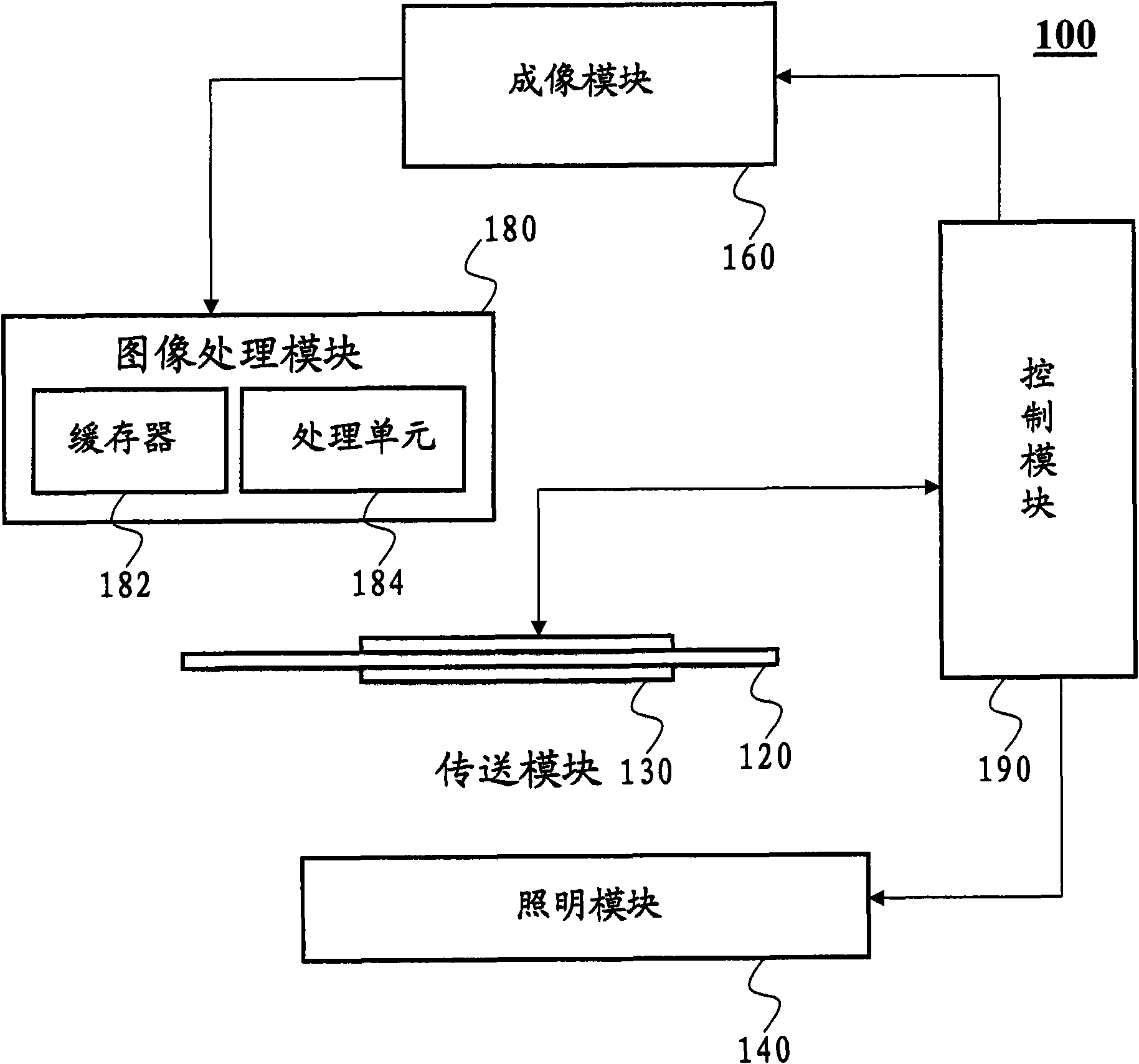
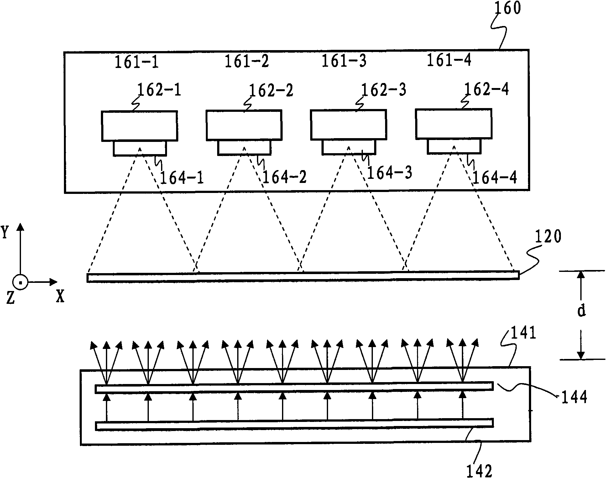
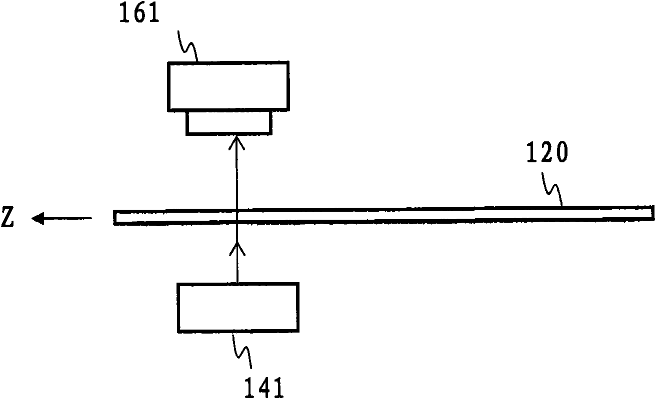
[0030] It should be understood that the drawings and description of the present invention have been simplified to illustrate elements useful in a clear understanding of the present invention, while other elements of a typical defect detection system have been removed for the purpose of clarity. Those skilled in the art will recognize that other elements may be desirable and / or necessary in order to practice the invention. However, since these elements are well known in the art, and since they do not contribute to a better understanding of the present invention, no description is given herein regarding these elements. It should also be understood that the drawings included herein merely give diagrammatic representations of current embodiments of the invention and that structures falling within the scope of the invention may include structures other than those shown in these drawings. In the drawings, similar structures are given similar reference numerals.

[0031] As mentione...


PUM


Abstract

The invention discloses a system and a method for detecting defect on or in a transparent or semitransparent patterned or structured substrate. The system comprises at least one imaging element, a first light source and a conveying device, wherein the at least one imaging element is used for scanning the substrate; the first light source is arranged close to the substrate for irradiating diffusedlight to the substrate; the first light source and the at least one imaging element form a first detection passage about the substrate; and the conveying device is used for producing relative movement between the substrate and the at least one imaging element as well as the first light source. In the invention, the patterned substrate is irradiated by using a short-distance diffusion mode so as to effectively eliminate the influence of the pattern or structure in the substrate on the original image, so that the defect is highlighted so as to easily and accurately identify and classify the local defect.

Description

technical field [0001] The present invention relates generally to methods and systems for detecting localized defects in substrates, and more particularly to optical methods and systems for detecting localized defects on or in transparent or translucent patterned or structured substrates. Background technique [0002] In the field of transparent or translucent substrates, as the market (for example, the solar module industry) further improves the functional requirements of substrates, patterned or structured substrates are more and more favored by consumers. The patterns or structures such as Pyramidal or other shapes. Product defect detection is an important tool for quality control. For example, in the glass manufacturing process, different types of defects occur, including for example surface defects such as scratches, dirt, open air bubbles, etc., and internal defects such as closed air bubbles, stones (including black stones, white stones, or stones of other colors) ....

Claims


Application Information

Patent Timeline
Patent Type & Authority Applications(China)
IPC IPC(8): G01N21/956G01N21/896
CPCG01N21/896G01N2021/8874G01N21/898G01N2021/8854H02S50/15Y02E10/50
Inventor 史伟杰李惠芬林晓峰郭峰郭晓锋
Owner SAINT-GOBAIN GLASS FRANCE
Why Eureka
Try Eureka