Optical element and method for making the same, master and method for making the same, and display apparatus

A technology of optical elements and structures, applied in the directions of optical elements, optics, diffusing elements, etc., can solve the problem of easy generation of stripes, and achieve the effect of high contrast, high anti-glare, and suppression of stripes.

Inactive Publication Date: 2010-09-01
SONY CORP
View PDF3 Cites 20 Cited by
  • Summary
  • Abstract
  • Description
  • Claims
  • Application Information

AI Technical Summary

Problems solved by technology

That is, since the structure of the optical element is regularly formed, the pixels of the display

Method used


Image

  • Optical element and method for making the same, master and method for making the same, and display apparatus
  • Optical element and method for making the same, master and method for making the same, and display apparatus
  • Optical element and method for making the same, master and method for making the same, and display apparatus

Examples


no. 1 example

[0082] (1) First embodiment (example of utilizing laser processing to make embossing roller):

[0083] (1.1) Structure of liquid crystal display device

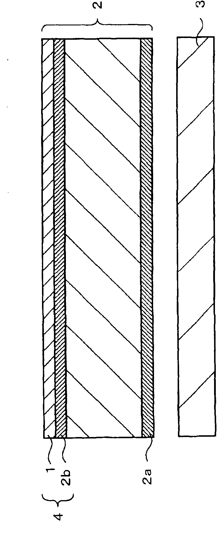
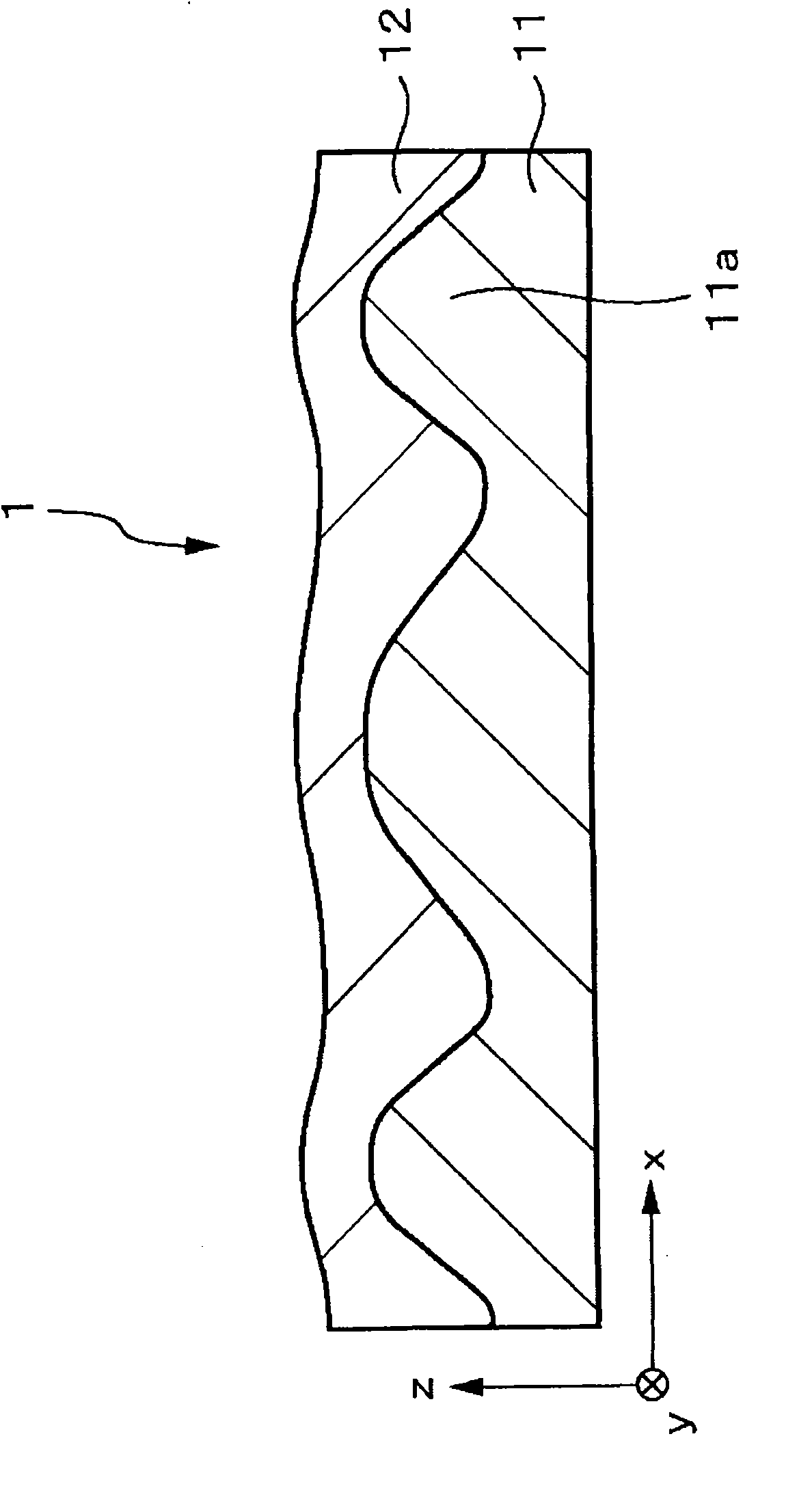
[0084] (1.2) Structure of optical film

[0085] (1.3) Embossing replication device

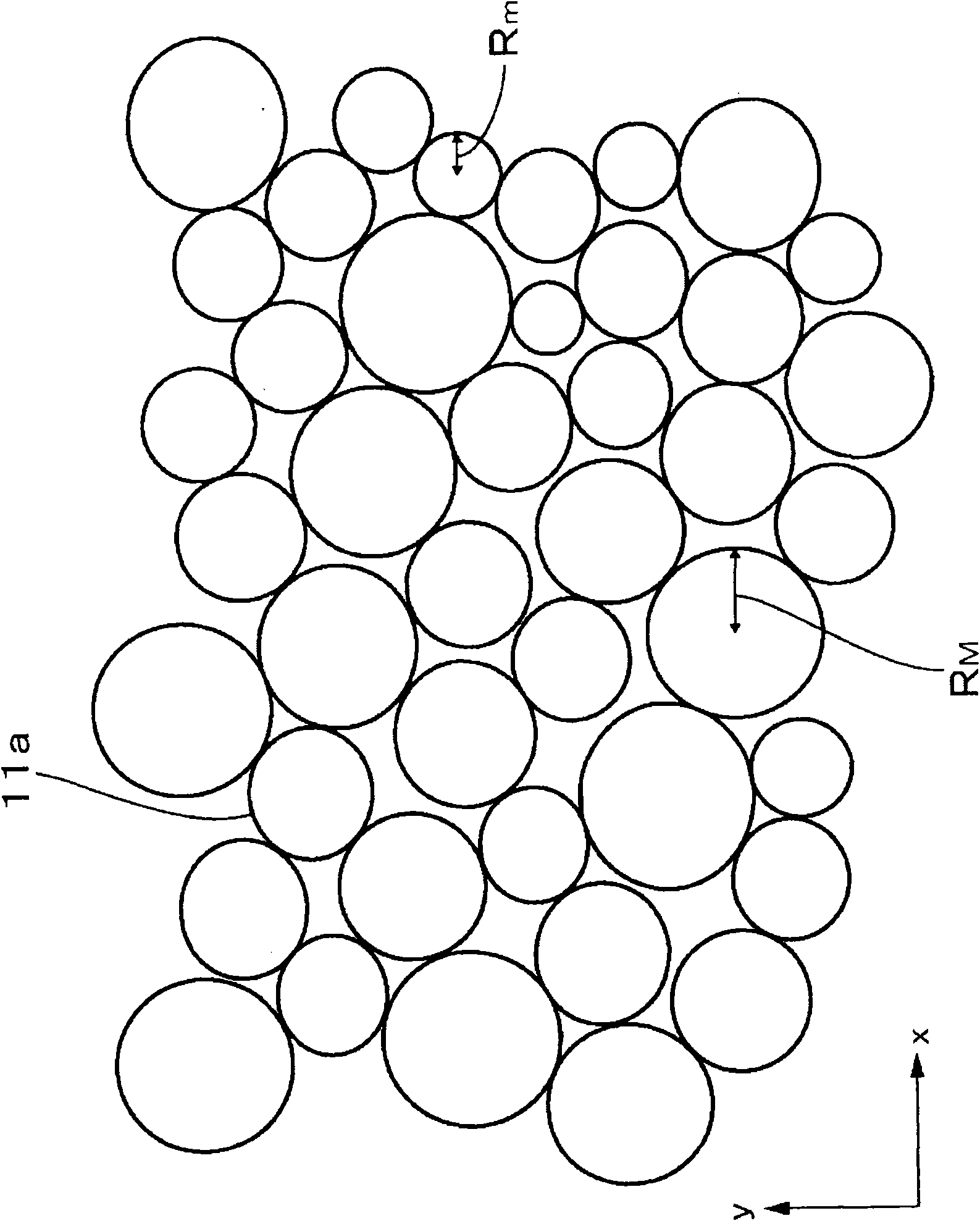
[0086] (1.4) Method of arranging circles on transfer rollers

[0087] (1.5) About random point generation algorithm

[0088] (1.5.1) Generation method of data on the X axis 1

[0089] (1.5.2) Generation method of data on the X-axis 2

[0090] (1.5.3) Circle filling method 1

[0091] (1.5.4) Circle filling method 2

[0092] (1.5.5) Tiling method

[0093] (1.6) Graphics generation device

[0094] (1.7) Manufacturing method of optical film

[0095] (2) Second Example (Example of Fabricating an Embossing Roll by Etching)

[0096] (3) Third embodiment (an example of further forming an antistatic layer)

[0097] (4) Fourth embodiment (an example in which an anti-reflection layer is further formed on the surface)

no. 5 example

[0098] (5) Fifth Embodiment (First Example of ANR Film)

no. 6 example

[0099] (6) Sixth Embodiment (Second Example of ANR Film)


PUM

PropertyMeasurementUnit
Ten point average roughnessaaaaaaaaaa
The average particle sizeaaaaaaaaaa
Thicknessaaaaaaaaaa

Abstract

An optical element and a method for making the same, a master and a method for making the same, and a display apparatus, which prevents generating stripe and has a high contrast and an antiglare property. An optical element includes a substrate including protruding structures on the surface and a hard coat layer formed on the substrate. An irregular shape is formed by the structures. An irregular shape resembling the irregular shape of the substrate is formed on a surface of the hard coat layer and is smoother than the that of the substrate. The size of bottoms of the structures changes at random within the range of the minimum distance Rm to the maximum distance Rm (Rm: minimum value of the shortest distance from the center of gravity of the bottom of the structure to the rim of the bottom, RM: maximum value of the longest distance from the center of gravity of the bottom of the structure to the rim of the bottom). Neighboring structures have bottoms in contact or substantially in contact with one another. Rm and Rm satisfy Rm /RM <= 0.9.

Description

technical field [0001] The present invention relates to an optical element and its manufacturing method, a master disc and its manufacturing method, and a display device. Specifically, it involves optical components with hard coatings. Background technique [0002] In recent years, various display devices such as liquid crystal displays (Liquid Crystal Displays: LCDs) and plasma displays (Plasma Display Panels: PDPs) have been widely used. The screens of these display devices are reflected by external light such as sunlight and indoor lighting, especially in bright places, and the visibility is significantly impaired. Therefore, optical films such as anti-glare films that diffuse and reflect external light are often used on the surface of the screen. . [0003] Conventionally, this optical film has used a method of forming a fine concavo-convex structure on the surface in order to diffuse and reflect external light on the surface of the screen. Specifically, the method of...

Claims


Application Information

Patent Timeline
IPC IPC(8): G02B5/02G03F7/00G03F1/00B32B3/28B32B7/02G02B1/10G02B1/118G02B1/14G02F1/1335
CPCG02B1/105G02B5/0294G02B5/0221G02F1/133502G02B1/118G02B1/11G02B5/0278G02B1/16A21C1/1485G02B1/14
Inventor 渡边仁内田厚石渡正之水野干久富永守雄大柳英树
Owner SONY CORP
Why Eureka
Try Eureka