Three-value FeRAM circuit
A ferroelectric memory and ferroelectric capacitor technology, applied in static memory, digital memory information, information storage, etc., can solve the problems of backward storage density and technological level, etc.
- Summary
- Abstract
- Description
- Claims
- Application Information
AI Technical Summary
Problems solved by technology
Method used
Image


Examples
Embodiment 1
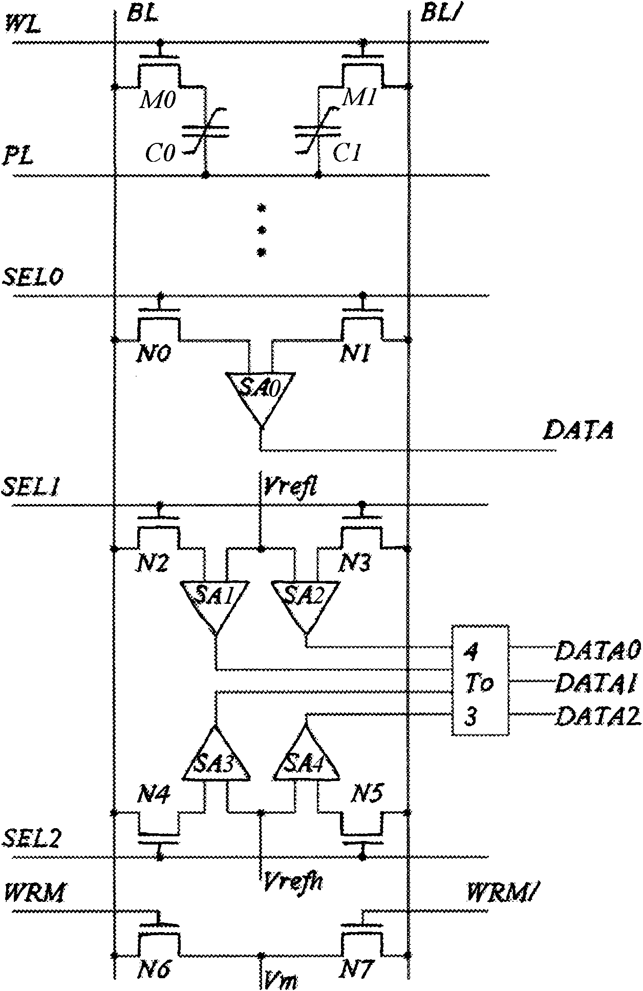
[0032] When performing a binary write operation, the timing is as follows Figure 4 As shown, the word line WL rises, the NMOS transistor is turned on, BL and BL / are the data to be written, the logic value "H" is written when the BL line is connected to a high level, and the logic value "H" is written when the BL line is connected to a low level. Logical value "L". Adding a pulse on PL, the polarization direction of the capacitor written in the logic value "H" and the capacitor written in the logic value "L" is always opposite. Finally, BL and BL / discharge, and the voltage returns to zero. The WL voltage returns to zero, the MOS tube is turned off, and the write operation ends.
Embodiment 2
[0034] When performing a binary read operation, the timing is as follows Figure 5 As shown, since the 2T2C memory cell structure is adopted, there is no need to generate a reference voltage separately, and the two input terminals of the sense amplifier SA0 are connected to BL and BL / respectively. The word line WL rises, and the NMOS transistor is turned on. At this time, although the remaining charges in the two ferroelectric capacitors are different, the BL and BL / voltage are 0, and the 1 unit and the 0 unit cannot be distinguished. Add a pulse to PL, and charge sharing will occur on the ferroelectric capacitor and the parasitic capacitor of BL. Since the values stored in the two capacitors are opposite, different capacitance values C 0 and C 1 , presenting different voltages V on BL and BL / 0 and V 1 . At this time, SEL0 rises to high level, the sense amplifier starts to work, and the voltage difference V 1 -V 0 amplified, the high voltage is pulled to V DD , l...
Embodiment 3
[0036]When performing a three-value write operation, the word line WL rises, the NMOS transistor is turned on, and the data to be written is on BL and BL / . When BL is connected to a high level, a logic value "H" is written, and when it is connected to a low level Then write a logic value "L", and write a logic value "M" when WRM~WRM / is high. The writing of "H" and "L" states is similar to writing "1" and "0" in traditional binary memory, as described above. For the intermediate state "M", a coercive voltage is required for biasing when writing. For the specific timing, see Image 6 .
[0037] When writing a ternary value, each bit line should need three control signals, that is, each pair of bit lines needs 6 control signals. The decoder can be implemented by a 3-8 decoder, and by properly selecting 6 bits in the output of the 3-8 decoder 8, the control of writing in the bit line can be realized.
PUM
 Abstract
Description
Claims
Application Information
 - R&D
- Intellectual Property
- Life Sciences
- Materials
- Tech Scout
- Unparalleled Data Quality
- Higher Quality Content
- 60% Fewer Hallucinations
Browse by: Latest US Patents, China's latest patents, Technical Efficacy Thesaurus, Application Domain, Technology Topic, Popular Technical Reports.
© 2025 PatSnap. All rights reserved.Legal|Privacy policy|Modern Slavery Act Transparency Statement|Sitemap|About US| Contact US: help@patsnap.com