Solar cell structure with integrated discrete by-pass diode

a solar cell and diode technology, applied in the direction of photovoltaics, electrical devices, semiconductor devices, etc., can solve the problems of limited voltage and current output of solar cells, solar cells, assembly difficulties, etc., and achieve the effect of small area and large area

US20050072457A1Active Publication Date: 2005-04-07THE BOEING CO
9 Cites 62 Cited by

Patent Information

Authority / Receiving Office
US · United States
Patent Type
Applications(United States)
Current Assignee / Owner
Publication Date
2005-04-07

Smart Images

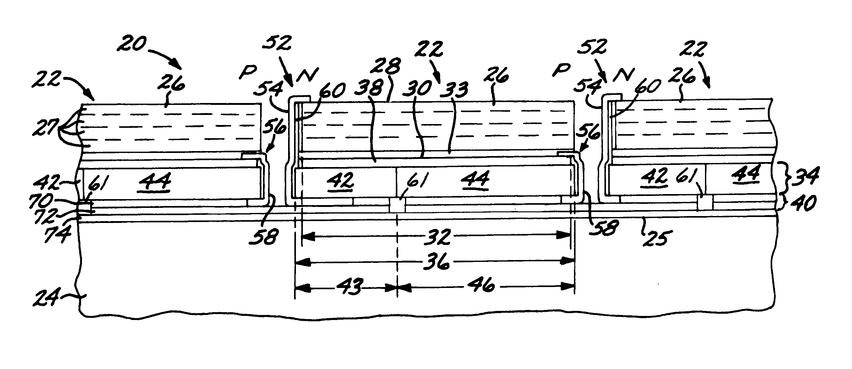
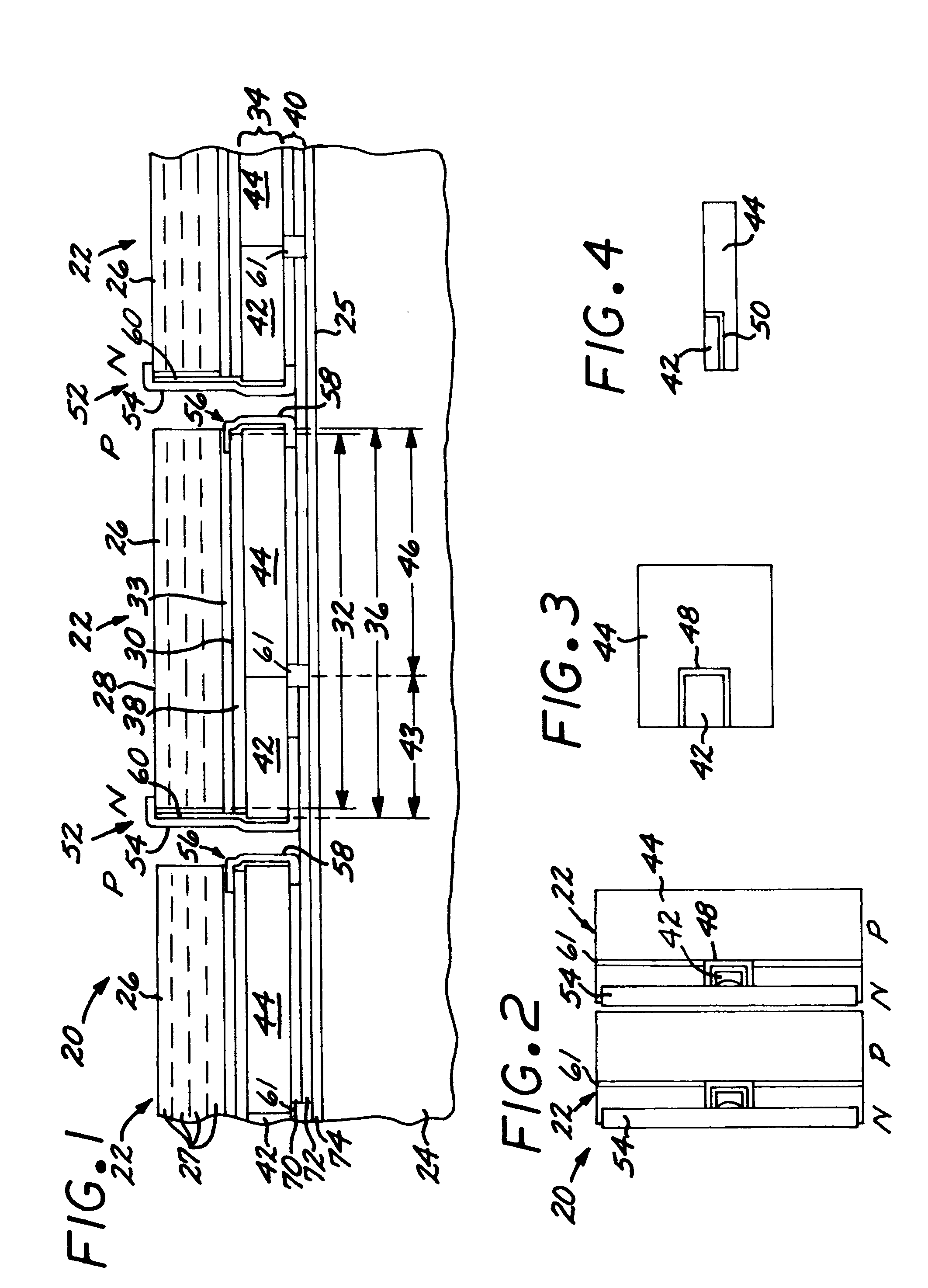
  • Figure 1
    Figure 1
  • Figure 2
    Figure 2
  • Figure 3
    Figure 3
Patent Text Reader

Abstract

A solar cell structure has a solar cell unit structure including a heat sink, and a solar cell having a front side, a back side, and a solar-cell projected area coverage on the heat sink. The solar cell has an active semiconductor structure that produces a voltage between the front side and the back side when the front side is illuminated. An intermediate structure is disposed between and joined to the back side of the solar cell and to the heat sink. The intermediate structure has an intermediate-structure projected area coverage on the heat sink and includes a by-pass diode having a diode projected area coverage on the heat sink. The diode projected area coverage on the heat sink may be substantially the same as the intermediate-structure projected coverage on the heat sink. Alternatively, the diode projected area coverage on the heat sink maybe less than the solar-cell projected area coverage on the heat sink, and the intermediate structure further includes a substrate coplanar with the by-pass diode.
Need to check novelty before this filing date? Find Prior Art

Description

[0001] This invention relates to solar cell structures and, more particularly, to a solar cell structure in which a discrete by-pass diode is integrated into the solar cell structure. BACKGROUND OF THE INVENTION

[0002] A solar cell is formed of two (or more) semiconductor layers in facing contact with each other at a semiconductor junction. When illuminated by the sun or otherwise, the solar cell produces a voltage between the semiconductor layers. Advanced solar cells may include more than two semiconductor layers and their respective pairwise semiconductor junctions. The various pairs of semiconductor layers of the advanced solar cells are tuned to the various spectral components of the sun to maximize the power output of the solar cell.

[0003] The voltage and current output of the solar cell are limited by the materials of construction and the surface area of the solar cell. Most commonly, a number of solar cells are electrically interconnected in series and / or parallel arrays to...

Examples

Embodiment Construction

[0023]FIGS. 1-2 depict a first embodiment of a solar cell structure 20. The solar cell structure 20 includes at least one, typically at least two, and in most cases a plurality of solar cell unit structures 22. Each solar cell unit structure 22 has a functional active semiconductor solar cell that produces a voltage between the front side and the back side when the front side is illuminated, but in most cases there are two or more of the solar cell unit structures 22 arranged in a series, parallel, or combined series / parallel array to produce the desired voltage and current outputs.

[0024] Each solar cell unit structure 22 includes a heat sink 24, and there may be (and usually are) more than one of the solar cell unit structures 22 on a single shared common heat sink 24, as illustrated. The heat sink 24 preferably has a substantially planar surface 25. The heat sink 24 is preferably made of a metal such as copper or aluminum, or a ceramic of good thermal conductivity such as aluminu...