Chemical vapor deposition device

A chemical vapor deposition and growth chamber technology, used in electrical components, semiconductor/solid-state device manufacturing, circuits, etc., can solve problems such as poor controllability, unfavorable process promotion, and increased productivity difficulty, to ensure stability, The effect of high growth efficiency and the most efficient growth

Active Publication Date: 2010-09-01
INST OF SEMICONDUCTORS - CHINESE ACAD OF SCI
View PDF1 Cites 1 Cited by
  • Summary
  • Abstract
  • Description
  • Claims
  • Application Information

AI Technical Summary

Problems solved by technology

[0006] Before the present invention, chemical vapor deposition devices, especially MOCVD devices, existed: they all used a single chamber to grow complex structures, including buffer layers, n-type contact layers, active layers, p-type contact layers, etc., and the growth cycle was longer, often requiring several One furnace is grown in more than one hour, and each manufacturer mainly achieves production capacity increase and cost reduction through the gradual expansion of multi-chip systems. This direction has encountered obvious bottlenecks, and it is gradually becoming more difficult to further expand production capacity. It is difficult to further improve production efficiency and Reduce the growth cost; n-type materials and p-type materials are grown in the same room. Due to the sensitivity of semiconductor materials to doping, the change of background concentration after a certain type of material is grown will directly affect the growth of the next type of material, and this The process is related to a specific growth history, and the controllability will be poor, which will seriously affect the repeatability of the equipment and make the role of human factors in the growth of the material prominent, resulting in the growth of the material varies from person to person and from time to time, which is not conducive to the process The popularization is therefore not conducive to the stable and repeatable realization of production

Method used


Image

  • Chemical vapor deposition device
  • Chemical vapor deposition device

Examples


Embodiment Construction

[0026] In order to make the object, technical solution and advantages of the present invention clearer, the present invention will be described in further detail below in conjunction with specific embodiments and with reference to the accompanying drawings.

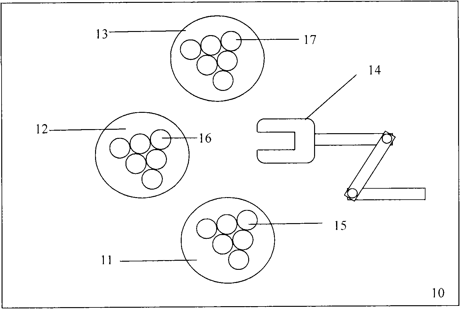
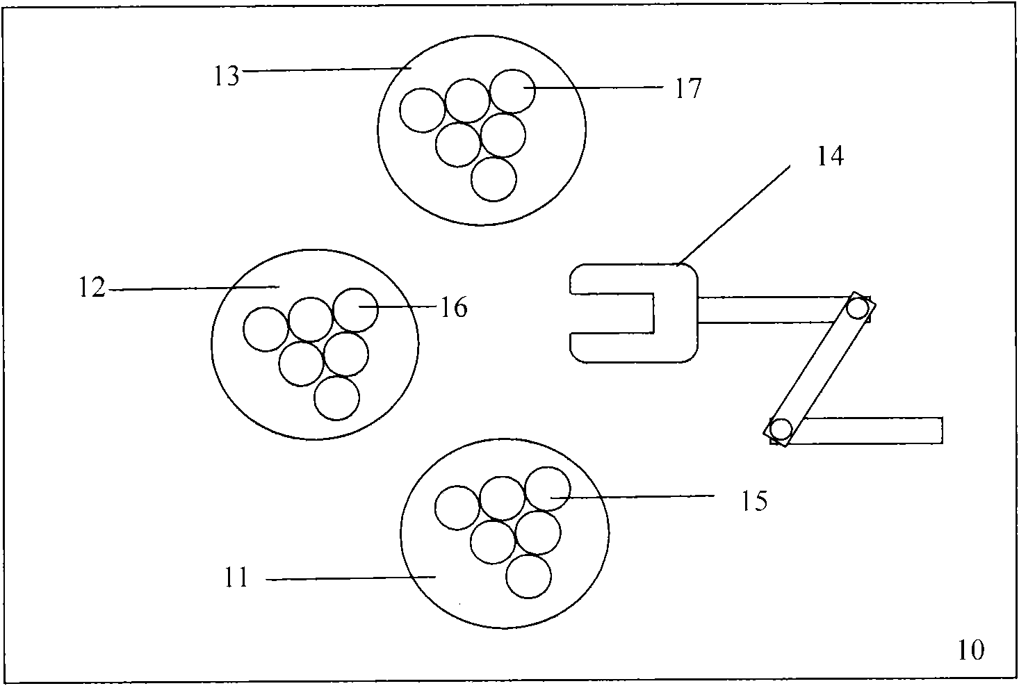
[0027] In order to achieve high reliability, low cost, and high efficiency growth of semiconductor epitaxial materials, we designed a chemical vapor deposition device, and built multiple reaction chambers in the device, and different reaction chambers grow different material structures.

[0028] by figure 1 For example, the chemical vapor deposition device designed by the present invention includes three independent reaction chambers, wherein reaction chamber 11 is dedicated to the growth of n-type layer epitaxial material (independent n-type layer epitaxial material growth chamber), and reaction chamber 12 is dedicated to active Layer growth (independent active layer growth chamber), the reaction chamber 13 is dedicated ...


PUM


Abstract

The invention discloses a chemical vapor deposition device, which comprises a plurality of independent growth chambers which are positioned in a tank body, use mechanical arms for conveying samples and are used for growing materials of different growing processes, such as n-type layer epitaxial materials, multiquantum well active layers, and p-type layer epitaxial materials. When the device is used, the problem that because the conventional chemical vapor deposition device, particularly MOCVD device, grows a structural material at one time in a single reaction room, the conventional chemical vapor deposition device is complex and the deposition process is complex, susceptible to various factors, low in repeatability, low in promotion property, long in process period and low in production efficiency, and other problems are solved.

Description

technical field [0001] The present invention relates to the field of semiconductor technology, and refers to a chemical vapor deposition device designed and manufactured to grow complex semiconductor epitaxial materials with high efficiency and high stability. By decomposing and growing complex structures, the maximum optimization and high repetition of a single process can be realized. , especially suitable for growing semiconductor complex epitaxial structures including n-type layers, active layers, p-type layers, etc. that may interact with each other, such as LED structures, LD structures, and PD structures. Background technique [0002] Semiconductor materials are necessary materials for the production of semiconductor devices and are the basis for the application of semiconductor devices. It determines and supports the level and development of the entire semiconductor electronic product. At present, the most important kind of semiconductor material is semiconductor epi...

Claims


Application Information

Patent Timeline
Patent Type & Authority Applications(China)
IPC IPC(8): H01L21/205
Inventor 段瑞飞曾一平王军喜冉军学胡国新羊建坤梁勇路红喜李晋闽
Owner INST OF SEMICONDUCTORS - CHINESE ACAD OF SCI
Why Eureka
Try Eureka