Method for improving electric conductivity of carbon nano tube network

A technology of carbon nanotubes and conductivity, which is applied in the field of improving the conductivity of carbon nanotube networks, can solve problems affecting the conductivity of carbon nanotube fibers, etc., and achieve the effect of improving conductivity and performance

Inactive Publication Date: 2010-09-15
SHANGHAI INST OF APPLIED PHYSICS - CHINESE ACAD OF SCI
View PDF0 Cites 3 Cited by
  • Summary
  • Abstract
  • Description
  • Claims
  • Application Information

AI Technical Summary

Problems solved by technology

This also affects the conductivity of

Method used


Image

  • Method for improving electric conductivity of carbon nano tube network
  • Method for improving electric conductivity of carbon nano tube network
  • Method for improving electric conductivity of carbon nano tube network

Examples


Embodiment 1

[0022] Specifically, proceed through the following steps:

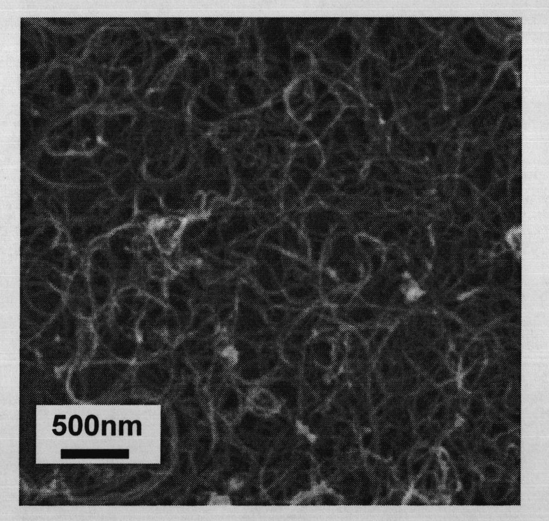
[0023] 1) Carbon nanotube sample preparation: carbon nanotube powder was put into ethanol solvent to prepare a suspension, and the water area was sonicated for 3 hours. The substrate is a flat, cleaned quartz plate of 20mm×20mm×1mm. The substrate is placed on a heating stage with a temperature of 150°C, covered with a 0.3mm thick mask to control the shape and size of the sample, and placed for 10 minute. Use a pneumatic airbrush to spray the prepared carbon nanotube suspension onto the heated substrate in the form of a spray with the assistance of nitrogen, and control the spraying time so that the transmittance of the resulting carbon nanotube network at 550nm visible light is 88%. %. Replace the substrate with a conductive silicon wafer, repeat the above preparation process, so that the carbon nanotube network on the silicon wafer is the same as that on the quartz substrate, observe the sample on the silicon wafer...

Embodiment 2

[0029] Specifically, proceed through the following steps:

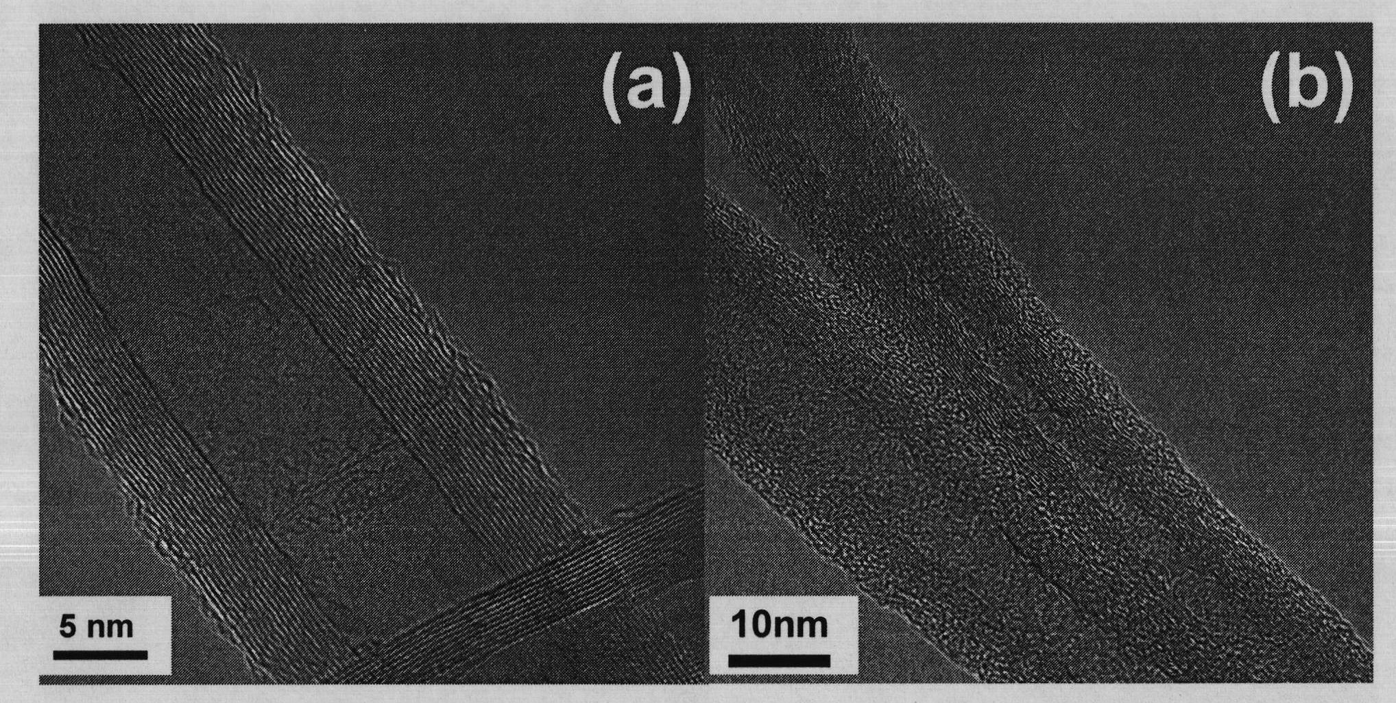
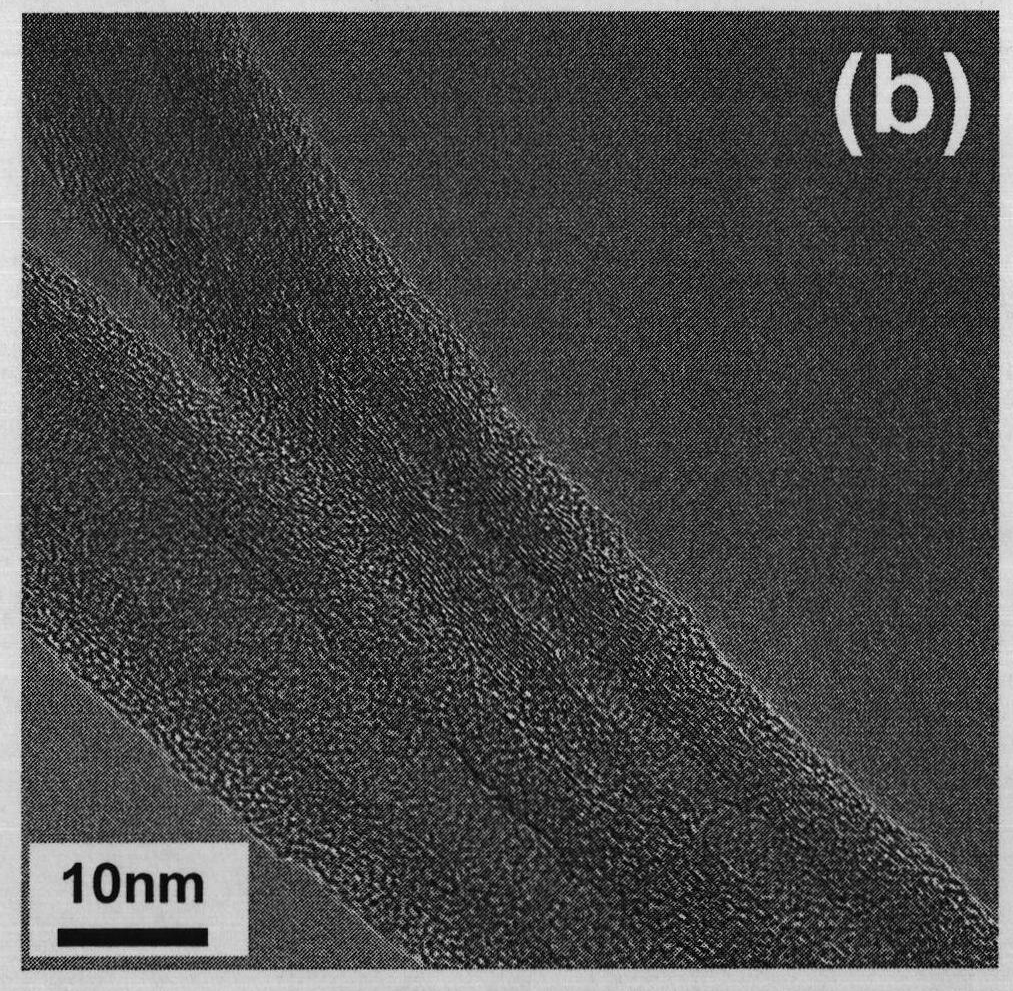
[0030] 1) Carbon nanotube sample preparation: carbon nanotube powder was put into ethanol solvent to prepare a suspension, and the water area was sonicated for 3 hours. The substrate is a flat, cleaned quartz plate of 20mm×20mm×1mm. The substrate is placed on a heating stage with a temperature of 150°C, covered with a 0.3mm thick mask to control the shape and size of the sample, and placed for 10 minute. Use a pneumatic airbrush to spray the prepared carbon nanotube suspension onto the heated substrate in the form of a spray with the assistance of nitrogen, and control the spraying time so that the transmittance of the resulting carbon nanotube network at 550nm visible light is 63%. %.

[0031] 2) Place the sample on the quartz substrate in a vacuum (vacuum degree 10 -4 Pa) was heated to 800K, kept for at least 30 minutes, and then naturally cooled to room temperature in vacuum. The conductivity of the network was...


PUM

PropertyMeasurementUnit
Conductivityaaaaaaaaaa

Abstract

The invention discloses a method for improving electric conductivity of a carbon nano tube network, which comprises the following steps of: (1) uniformly distributing carbon nano tubes on the surface of a substrate to form a sample; (2) placing the distributed carbon nano tube sample in a target chamber of an ion beam irradiation device, and heating the sample; (3) after the carbon nano tube sample is heated to a thermodynamic temperature of between 700 and 1,000 DEG C, irradiating the sample by using ion beams; and (4) after the irradiation is finished, stopping heating, and cooling the sample to room temperature, and taking the sample out of the target chamber. Compared with the prior art, the method can effectively improve the electric conductivity of the carbon nano tube network under the condition of avoiding chemical pollution, can be compatible with the conventional semiconductor process, and can be used for promoting the performance of carbon nano tube related devices and used for manufacturing flexible transparent conductive films of the carbon nano tubes.

Description

technical field [0001] The invention relates to a method for improving the conductivity of the carbon nanotube network. Background technique [0002] Since their discovery in 1991, carbon nanotubes have attracted great attention due to their excellent properties in electricity, heat, and mechanics. One of the application forms of carbon nanotubes is that multiple carbon nanotubes are aggregated into a network or film, which is generally soft, transparent and conductive. Although metallic carbon nanotubes themselves have good electrical conductivity, when they overlap to form a network, since adjacent carbon nanotubes only interact with each other by Van der Waals force, the contact resistance between the tubes is caused. Larger, which limits the conductivity of macroscopic carbon nanotube films. [0003] The currently reported methods to improve the conductivity of carbon nanotube films are mainly to disperse the carbon nanotubes with surfactants (such as sodium lauryl sul...

Claims


Application Information

Patent Timeline
IPC IPC(8): C01B31/02
Inventor 周广颖闫隆
Owner SHANGHAI INST OF APPLIED PHYSICS - CHINESE ACAD OF SCI
Why Eureka
Try Eureka