Supercharge Your Innovation With Domain-Expert AI Agents!

Horizontal electric field type liquid crystal display device and manufacturing method thereof

A technology of a liquid crystal display device and a horizontal electric field, which is applied in the field of microelectronics, can solve the problems that the horizontal electric field type liquid crystal display device cannot increase the aperture ratio, etc., and achieve the effects of reducing the horizontal distance, increasing the area, and reducing the manufacturing cost

Active Publication Date: 2010-09-15
BOE TECH GRP CO LTD +1
View PDF0 Cites 14 Cited by
  • Summary
  • Abstract
  • Description
  • Claims
  • Application Information

AI Technical Summary

Problems solved by technology

[0012] The purpose of the present invention is to provide a horizontal electric field type liquid crystal display device and a manufacturing method, to overcome the defect that the technique of increasing the aperture ratio cannot be adopted in the horizontal electric field type liquid crystal display device in the prior art

Method used


Image

  • Horizontal electric field type liquid crystal display device and manufacturing method thereof
  • Horizontal electric field type liquid crystal display device and manufacturing method thereof
  • Horizontal electric field type liquid crystal display device and manufacturing method thereof

Examples


no. 1 example

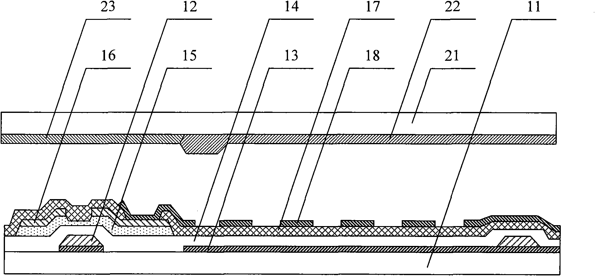
[0069] figure 2 It is a schematic diagram of the first embodiment of the horizontal electric field liquid crystal display device of the present invention. Such as figure 2 As shown, the liquid crystal display device of this embodiment includes: a first substrate 11, a second substrate 21, and a liquid crystal layer sandwiched between the first substrate and the second substrate, wherein,

[0070] The first substrate 11 includes: a plurality of thin film transistors, gate lines and data lines for driving the plurality of thin film transistors; the second substrate 21 includes: a plurality of pixel electrodes 18 and corresponding to the pixel electrodes 18 and a common electrode 13 forming a horizontal electric field; and the liquid crystal display device further includes: a plurality of conductive spacers 24 for electrically connecting each of the pixel electrodes and each of the thin film transistors respectively.

[0071] In the liquid crystal display device of this embod...

no. 4 example

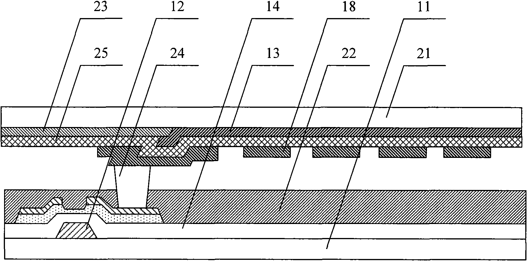
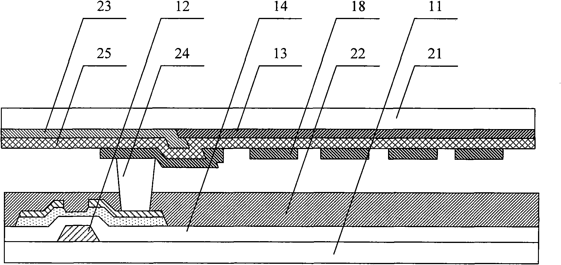
[0088] Figure 5 It is a schematic diagram of the fourth embodiment of the horizontal electric field type liquid crystal display device of the present invention. Such as Figure 5 As shown, the liquid crystal display device of this embodiment includes: a first substrate 11 and a second substrate 21, and the first substrate 11 includes: a thin film transistor located on the first substrate 11, a black matrix 23 located on the thin film transistor, and a color The resin 22 is located on the black matrix 23, and the drain electrode of the thin film transistor is provided with a colored resin via hole and a black matrix via hole; the second substrate 21 includes: the common electrode 13 is located on the second substrate 21, the second An insulating layer is located on the common electrode 13, the pixel electrode 18 is located on the first insulating layer 25 and has at least one gap, and a conductive spacer 24 is located on the pixel electrode 18 for electrically connecting the ...

no. 5 example

[0142] Figure 10a It is a flow chart of the fifth embodiment of the manufacturing method of the horizontal electric field type liquid crystal display device of the present invention. Figure 10b It is a schematic diagram of forming a thin film transistor in the fifth embodiment of the method for manufacturing a horizontal electric field type liquid crystal display device of the present invention. Figure 10c It is a schematic diagram of forming colored resin in the fifth embodiment of the method for manufacturing a horizontal electric field type liquid crystal display device of the present invention. Figure 10d It is a schematic diagram of forming a black matrix and a common electrode in the fifth embodiment of the method for manufacturing a horizontal electric field type liquid crystal display device of the present invention. Figure 10e It is a schematic diagram of depositing the first insulating layer in the fifth embodiment of the manufacturing method of the horizontal ...


PUM


Abstract

The invention relates to a horizontal electric field type liquid crystal display device and a manufacturing method thereof. The horizontal electric field type liquid crystal display device comprises a first substrate, a second substrate, a liquid crystal layer clamped between the first and second substrates and a plurality of conductive insulators, wherein the first substrate comprises a plurality of thin film transistors, grid lines for driving the plurality of thin film transistors and data wires; the second substrate comprises a plurality of pixel electrodes and public electrodes which are correspond to the pixel electrodes and form a horizontal electric field; and the conductive insulators are used for electrically connecting the pixel electrodes and the thin film transistors respectively. The liquid crystal display device of the embodiment overcomes the drawbacks of the prior art by arranging the thin film transistors on the first substrate and forming the public electrodes and the pixel electrodes on the second substrate.

Description

technical field [0001] The invention belongs to the field of microelectronics, in particular to a horizontal electric field type liquid crystal display device and a manufacturing method. Background technique [0002] A liquid crystal display device (Liquid Crystal Display, referred to as LCD) is a main flat panel display device (Flat Panel Display, referred to as FPD). [0003] Liquid crystal display devices are classified into vertical electric field type liquid crystal display devices and horizontal electric field type liquid crystal display devices according to the direction of an electric field for driving liquid crystals. Vertical electric field type liquid crystal display devices include: twisted nematic (Twist Nematic, referred to as TN) type liquid crystal display devices; horizontal electric field type liquid crystal display devices include: boundary field switching (Fringe Field Switching, referred to as FFS) type liquid crystal display devices In-Plane Switching ...

Claims


Application Information

Patent Timeline
IPC IPC(8): G02F1/1343G02F1/1333G02F1/1362
CPCG02F1/13394G02F2001/13398G02F1/134363G02F1/13398
Inventor 闵泰烨裴扬王静高文宝
Owner BOE TECH GRP CO LTD
Features
  • R&D
  • Intellectual Property
  • Life Sciences
  • Materials
  • Tech Scout
  • Unparalleled Data Quality
  • Higher Quality Content
  • 60% Fewer Hallucinations
Learn More