Duty ratio calibration circuit of precharge logical digital clock

A digital clock and calibration circuit technology, applied in the direction of transforming continuous pulse chains into pulse chain devices with required modes, etc., can solve problems such as long settling time, change influence, small edge jitter, etc.

CN101834587AInactive Publication Date: 2010-09-15SOUTHEAST UNIV
0 Cites 8 Cited by

Patent Information

Authority / Receiving Office
CN · China
Patent Type
Applications(China)
Current Assignee / Owner
Publication Date
2010-09-15
Estimated Expiration
Not applicable · inactive patent

Smart Images

  • Figure 1
    Figure 1
  • Figure 2
    Figure 2
  • Figure 3
    Figure 3
Patent Text Reader

Abstract

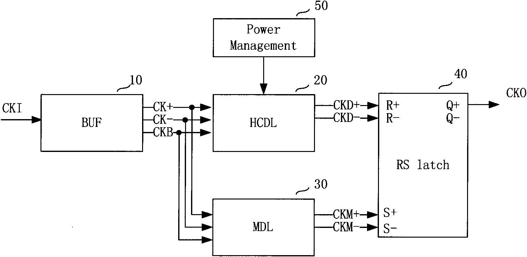
The invention discloses a duty ratio calibration circuit of a precharge logical digital clock, which comprises an input buffer stage BUF, a cycle delay line HCDL, a matching delay line MDL, a RS trigger and a power control module PM. The duty ratio calibration circuit of the invention has the advantages of rapid establishment (1.5 clock cycles), relative stability and no accumulative effect of duty ratio calibration errors. Compared with some duty ratio calibration circuits based on digital detection and adjustment mode, differential precharge logic is adopted in the invention to construct a basic delay unit, so that the calibration circuit of the invention has smaller delay time, thereby obviously improving the upper limit of the working frequency of the circuit and the calibration accuracy. In the invention, the RS trigger with a novel structure is used for realizing more accurate matching of time delay of paths from a setting end to an output end and from a resetting end to the output end and keeping consistent characteristics under the condition of each technological angle.
Need to check novelty before this filing date? Find Prior Art

Description

technical field

[0001] The invention is mainly used in high-speed data communication systems and digital signal processing systems (such as high-speed data storage, pipeline processors, etc.) to correct the duty cycle of the system clock, and belongs to the technical field of duty cycle calibration circuit design. Background technique

[0002] With the advancement of integrated circuit technology, the main frequency of modern digital systems has been continuously increased, and technologies such as double data rate (DDR) and pipelines have been widely used to obtain greater data throughput. Therefore, the digital system also puts forward higher requirements on the signal quality of the working clock. A high-quality clock signal should have the characteristics of fast establishment, low jitter, and low skew, and a 50% duty cycle to ensure that the relevant timing constraints of data signal establishment and retention during transmission are met, and the system can be stable. ...

Examples

Embodiment Construction

[0036] The present invention will be described in detail below in conjunction with the accompanying drawings and specific examples.

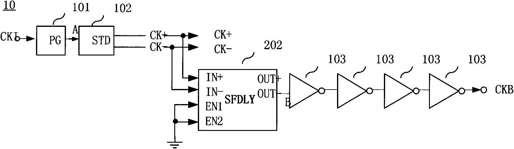
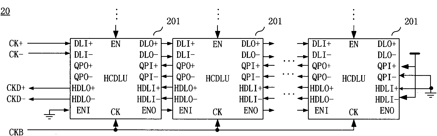
[0037] Such as figure 1 As shown, a digital clock duty ratio calibration circuit is characterized in that the left signal input terminal of the input stage 10 in the circuit receives the original input clock signal CKI calibrated; the output signal of the first and second signal output terminals of the input stage 10 The clock signals CK+ and CK- are respectively in differential form, and the output signal of the third signal output terminal is the buffered clock signal CKB. The buffered clock signal CKB is simultaneously connected to the corresponding input ends of the half-period delay line HCDL 20 and the matching delay line MDL 30; the output signal of the half-period delay line HCDL 20 is the half-period delayed clock signal CKD+ and CKD- in differential form, and The output signal of the matching delay line 30, that is, the matching delay...