Method for manufacturing semiconductor device

A manufacturing method and semiconductor technology, applied in semiconductor/solid-state device manufacturing, electrical components, circuits, etc., can solve problems such as increased thermal budget, sensitivity of wafer fluctuation devices, and unstable temperature peaks

Inactive Publication Date: 2010-09-22
SEMICON MFG INT (SHANGHAI) CORP
View PDF0 Cites 4 Cited by
  • Summary
  • Abstract
  • Description
  • Claims
  • Application Information

AI Technical Summary

Problems solved by technology

However, after the Wafer Acceptance Test (WAT), it was found that the application of spike annealing, due to the high peak temperature, enhanced the thermal budget of the process, causing polysilicon depletion (poly-depletion), resulting in wafer fluctuations and The sensitivity of the devic

Method used


Image

  • Method for manufacturing semiconductor device
  • Method for manufacturing semiconductor device
  • Method for manufacturing semiconductor device

Examples


Embodiment Construction

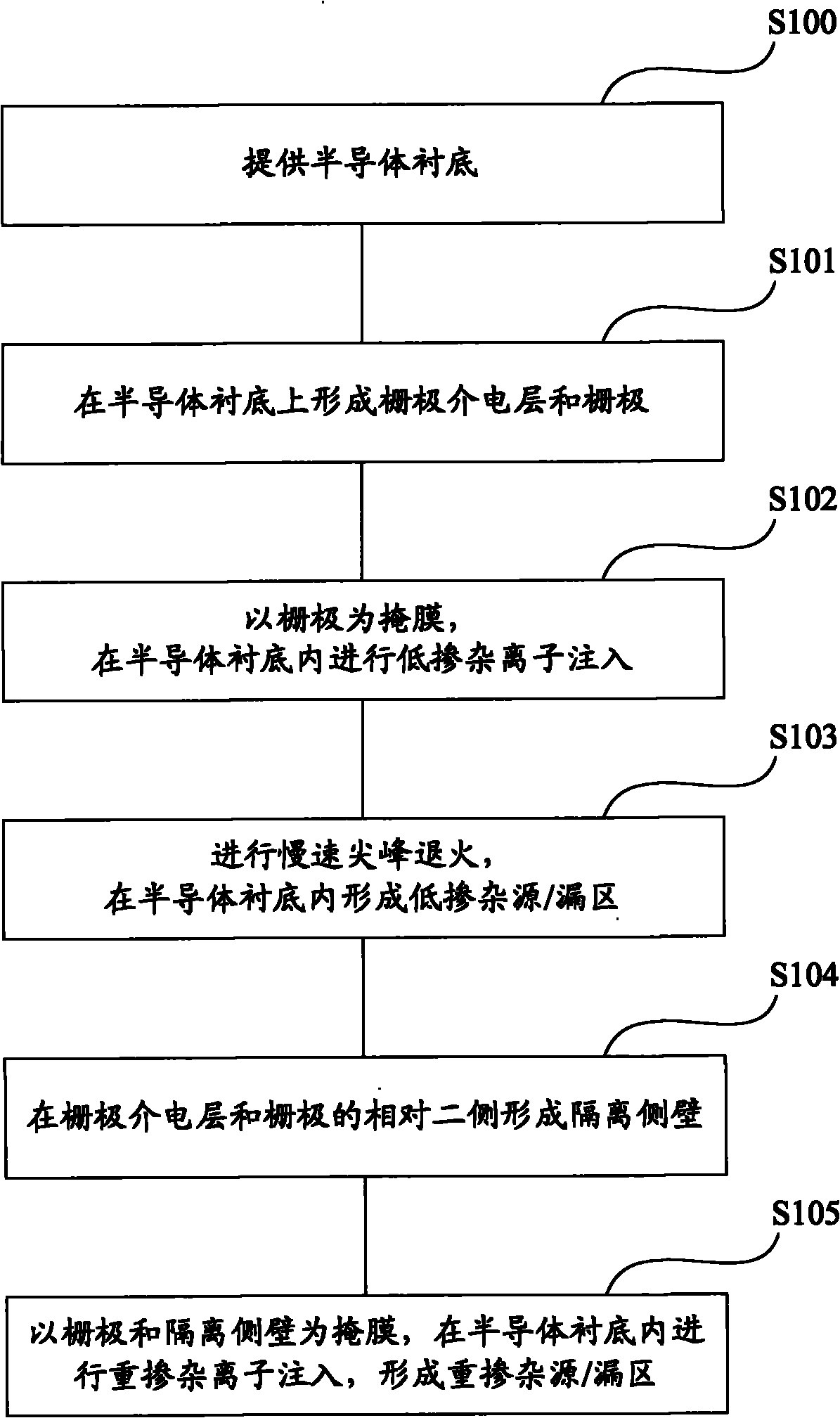
[0018] The inventors of the present invention have found that in the existing rapid thermal annealing process for suppressing the diffusion and migration of dopant ions, the effect of the peak annealing process on inhibiting the diffusion and migration of dopant ions is more obvious than that of the uniform temperature annealing process , but the spike annealing process will cause quality problems such as wafer fluctuations and device sensitivity degradation due to factors such as excessively high temperature peaks and excessively fast heating or cooling speeds.

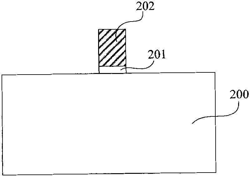
[0019] Therefore, in the manufacture of semiconductor devices, in order to prevent the occurrence of the above-mentioned defects. The present invention firstly provides a semiconductor substrate, on which a gate dielectric layer and a gate located on the gate dielectric layer are formed; using the gate as a mask, lightly doped with ions in the semiconductor substrate Implantation; performing slow spike annealing to f...


PUM


Abstract

The invention relates to a method for manufacturing a semiconductor device. The method comprises the following steps of: providing a semiconductor substrate, and forming a grid dielectric layer on the semiconductor substrate and a grid on the grid dielectric layer; taking the grid as a mask, and carrying out light-doping ion injection in the semiconductor substrate; carrying out slow spike-anneal, and forming a light-doping source/drain area in the semiconductor substrate; forming isolation side walls on two opposite sides of the grid dielectric layer and the grid; taking the grid and the isolation side walls as the masks, and carrying out heavy-doping ion injection in the semiconductor substrate to form a heavy-doping source/drain area. Compared with the prior art, the invention not only has the effects of activating doped elements and inhibiting the diffusion of the doped ions, but also can decrease the temperature fluctuation of the wafer, decrease the heat budge and enhance the sensitivity of the device.

Description

technical field [0001] The invention relates to the technical field of semiconductor manufacturing, in particular to a manufacturing method of a semiconductor device. Background technique [0002] With the rapid development of semiconductor manufacturing technology, in order to achieve faster computing speed, larger data storage capacity and more functions, semiconductor chips are developing towards high integration. The peripheral circuits of most semiconductor chips need to use high-voltage input / output devices, while core devices such as various storage devices need to operate at low voltage. In order to maximize device performance, the channel length of core devices is shortened, resulting in short Channel region and short channel effects. In order to avoid the short channel effect, a lightly doped source / drain (LDD) structure is usually used, but due to the diffusion and penetration of implanted ions in the source / drain region, it will cause the junction of the source / ...

Claims


Application Information

Patent Timeline
IPC IPC(8): H01L21/336H01L21/324H01L21/265
Inventor 赵猛
Owner SEMICON MFG INT (SHANGHAI) CORP
Why Eureka
Try Eureka