Method for manufacturing high-AR and fine-line PCB

A technology of fine lines and PCB boards, applied in the directions of printed circuit manufacturing, printed circuits, electrical components, etc., can solve the problems of difficulty and inability to manufacture, and achieve the effect of reducing the thickness of surface copper, facilitating manufacture, and reducing the difficulty of etching

Inactive Publication Date: 2010-09-22
CHINA CIRCUIT TECH SHANTOU CORP
View PDF4 Cites 34 Cited by
  • Summary
  • Abstract
  • Description
  • Claims
  • Application Information

AI Technical Summary

Problems solved by technology

Due to the contradiction between the surface copper thickness requirements and the hole copper thickness requirements, for the production of high thickness-to-diameter ratio and fine circuit PCB

Method used


Image

  • Method for manufacturing high-AR and fine-line PCB
  • Method for manufacturing high-AR and fine-line PCB

Examples


Embodiment Construction

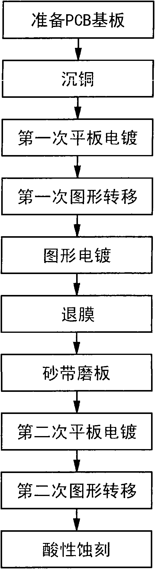
[0024] As shown in the accompanying drawings, the manufacturing method of high thickness-to-diameter ratio and fine circuit PCB board in this preferred embodiment includes the following steps:

[0025] (1) Prepare the PCB substrate: metallized holes are provided on the above PCB substrate;

[0026] (2) Copper sinking: perform copper sinking treatment on the PCB substrate according to the conventional copper sinking process;

[0027] (3) The first flat plate electroplating: The PCB substrate after the copper sinking treatment is immersed in the electroplating solution for electroplating. The surface copper thickness and the hole copper thickness of the first flat plate electroplating are both between 5 μm and 8 μm; the first flat plate The current density of electroplating is 1.2ASD, and the electroplating time is 21MIN;

[0028] The surface copper thickness and hole copper thickness of 5μm-8μm above can withstand various treatments in the subsequent manufacturing process;

...


PUM

PropertyMeasurementUnit
Thicknessaaaaaaaaaa

Abstract

The invention provides a method for manufacturing a high-AR (aspect ratio) and fine-line PCB (printed circuit board), which comprises the following steps: (1) preparing a PCB substrate; (2) carrying out PTH (plating through hole) process; (3) carrying out primary electroplating process; (4) carrying out primary pattern transfer; (5) carrying out pattern electroplating process; (6) removing dry film; (7) abrading the PCB substrate by an abrasive belt; (8) carrying out secondary electroplating process; (9) carrying out secondary pattern transfer; and (10) carrying out the acid etching process. By adopting the primary electroplating process and the secondary electroplating process and adopting the step for plating holes instead of surfaces with copper, the method of the invention can meet the requirements for the thickness of the hole copper, reduce the thickness of the surface copper and make the etching process easier at the same time, thus favoring for the production of fine-line and small-gap PCBs, being helpful for the fine-line manufacture and meeting the requirements of quality for the reliability of the PCBs.

Description

technical field [0001] The invention relates to a method for manufacturing a PCB board, more specifically, to a method for manufacturing a PCB board with a high thickness-to-diameter ratio and fine circuits. Background technique [0002] With the rapid development of electronic products, PCB boards (ie printed circuit boards) have entered the era of high aspect ratio (AR) and fine lines. The above-mentioned high aspect ratio generally means that the aspect ratio is greater than or equal to 8:1. [0003] In the production process of high thickness-to-diameter ratio and fine circuit PCB boards, the production of thin circuit and small-pitch PCB boards requires the surface copper thickness to be limited to a certain thickness. Beyond this thickness, the production of circuits will be difficult; and circuit boards The hole copper thickness has a minimum thickness requirement, which leads to a contradiction between the surface copper thickness requirement and the hole copper thic...

Claims


Application Information

Patent Timeline
IPC IPC(8): H05K3/00H05K3/18
Inventor 李国有黄志东苏维辉杨晓新郑惠芳苏启能蔡桂龙杨海永谢少英郑国光苏藩春谢伟明
Owner CHINA CIRCUIT TECH SHANTOU CORP
Why Eureka
Try Eureka