

Method for manufacturing printed circuit board
A technology of printed circuit boards and manufacturing methods, which is applied in the direction of removing conductive materials by chemical/electrolytic methods, which can solve the problems of excessive photoresist ink and the inability to fully wash off photoresist ink, and achieve cost-saving effects
- Summary
- Abstract
- Description
- Claims
- Application Information
AI Technical Summary
Problems solved by technology
Method used
Image

Examples
Embodiment 1
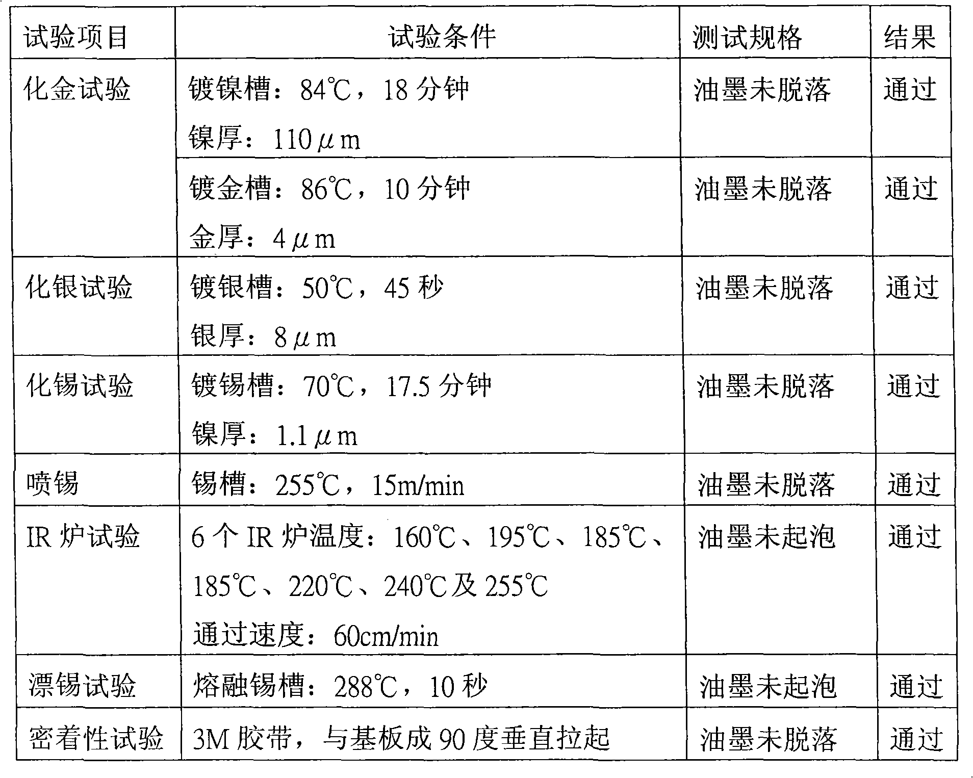
[0023] The ink used in this embodiment is NSR-1000 FG4 green ink purchased from Taiwan Jingnai Co., Ltd., which consists of dipropylene glycol monomethyl ether <10% by weight, dipropylene glycol monomethyl ether acetate <15% by weight , epoxy acrylic resin < 35% by weight, high boiling point aromatic naphtha < 5% by weight, acetophenone derivative photosensitizer < 10% by weight and barium sulfate < 30% by weight, and the viscosity of the ink after stirring is 80Pda.
[0024] On the copper foil with a thickness of 0.16cm, use the ink-covering knife or scraper respectively at a speed of 15cm / min and a pressure of 5kg / cm 2 , Apply the above ink to the c-side of the copper foil (the surface for mounting parts) at an angle of 15 degrees so as to have a thickness of 15 μm, and apply the above-mentioned ink to a thickness of 14 μm on the surface opposite to the c-side (referred to as the s-side) . Pre-bake at a temperature of 72°C for 10 minutes, with a photomask with the desired p...
PUM
| Property | Measurement | Unit |
|---|---|---|
| Thickness | aaaaa | aaaaa |
Abstract
Description
Claims
Application Information