

Vertical launching quantum cascade laser structure
A quantum cascade and vertical emission technology, applied to lasers, laser components, semiconductor lasers, etc., can solve problems such as difficult material growth and complex etching processes
- Summary
- Abstract
- Description
- Claims
- Application Information
AI Technical Summary
Problems solved by technology
Method used
Image

Examples
Embodiment Construction
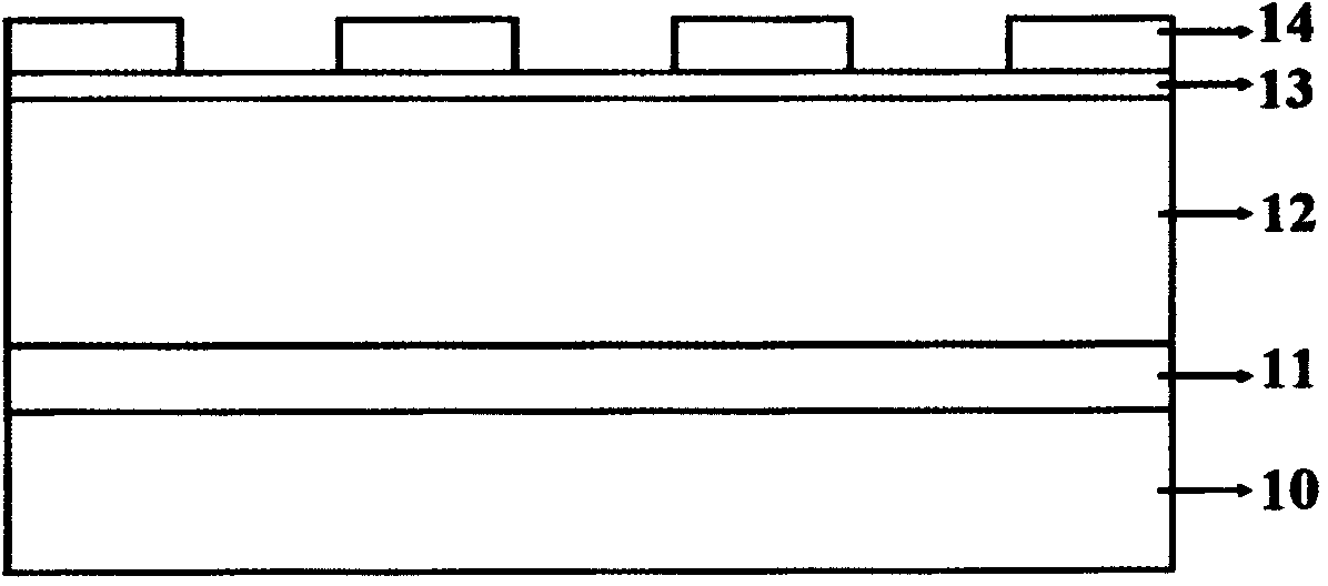
[0020] Please refer to the figure, the present invention provides a vertical emission quantum cascade laser structure, including:
[0021] A substrate 10, on which a waveguide layer 11, an active layer 12 and a contact layer 13 are grown sequentially; the substrate 10 is an InP substrate; the material of the waveguide layer 11 is InGaAs, the The waveguide layer 11 is n-type doped with a doping concentration of 6×10 16 cm -3 , with a layer thickness of 0.55 μm; the active layer 12 is composed of 40 cycles of InGaAs / InAlAs, and the wavelength corresponding to the active layer is 8-12 μm; the material of the contact layer 13 is InGaAs, and the doping concentration is 1×10 19 cm -3 , the layer thickness is 0.05 μm;
[0022] Metal grating layer 14, the metal grating layer 14 is located above the contact layer 13, and the metal grating layer 14 has a second-order Bragg period; the material of the metal grating layer 14 is silver, and the thickness of the metal grating layer 14 i...
PUM
 Abstract
Description
Claims
Application Information