Organic light emitting diode display

A light-emitting diode and display technology, which is applied in the direction of organic semiconductor devices, instruments, electric solid devices, etc., can solve problems such as degraded image quality, achieve the effects of improving visibility and image quality, avoiding reflection, and reducing total thickness

Inactive Publication Date: 2010-10-06
SAMSUNG DISPLAY CO LTD
View PDF0 Cites 41 Cited by
  • Summary
  • Abstract
  • Description
  • Claims
  • Application Information

AI Technical Summary

Problems solved by technology

Such Newton's rings can degrade the qual

Method used


Image

  • Organic light emitting diode display
  • Organic light emitting diode display
  • Organic light emitting diode display

Examples


Embodiment Construction

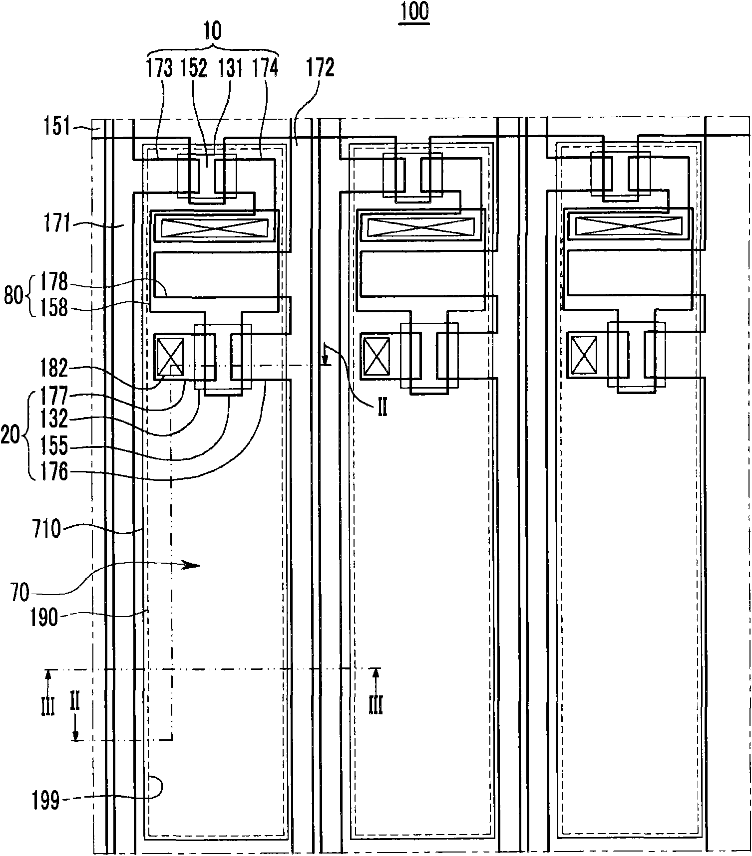
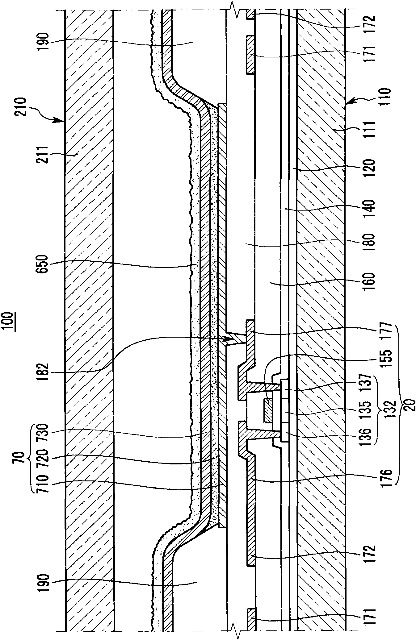
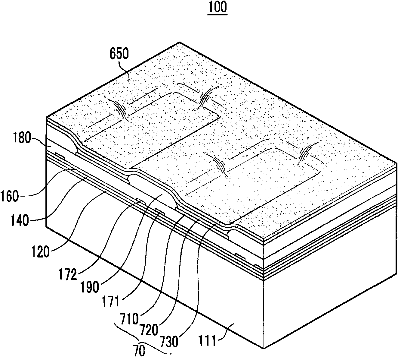
[0016] Embodiments of the present invention will now be described more fully hereinafter with reference to the accompanying drawings. As those skilled in the art would realize, the described embodiments may be modified in any different ways, all without departing from the spirit or scope of the present invention.

[0017] In order to clearly describe the embodiments of the present invention, structural parts irrelevant to the description may be omitted, and like reference numerals denote like elements throughout the specification. Also, the size and thickness of the respective structural components shown in the drawings are arbitrarily set for convenience of description, and the embodiments of the present invention are not necessarily limited to the illustrated mode.

[0018] In the drawings, the thickness of layers, films, panels, regions, etc., are exaggerated for clarity, better understanding, and convenience of illustration. It will be understood that when an element such...


PUM


Abstract

Embodiments provide an organic light emitting diode display. The display includes a substrate, a pixel electrode formed on the substrate, and an organic emissive layer formed on the pixel electrode. A common electrode is formed on the organic emissive layer. In addition, a crystallized light scattering layer is formed on the common electrode. The crystallized light scattering layer may be a crystallized organic or crystallized inorganic layer having a rough surface in order to effectively scatter light and prevent phenomenon, such as Newton's Rings from occurring in the display.

Description

technical field [0001] The present invention relates to an organic light emitting diode display, and more particularly, to an organic light emitting diode display having improved visibility and image quality. Background technique [0002] An organic light emitting diode (OLED) display generally has a plurality of organic light emitting diodes, each of which has a hole injection electrode, an organic emissive layer, and an electron injection electrode. In organic light emitting diode displays, electrons and holes generally recombine with each other in an organic emission layer, thereby generating excitons. When the excitons are transferred from an excited state to a ground state, energy is generated to emit light, and an image can be displayed based on the emitted light. [0003] Therefore, organic light emitting diode displays generally involve emissive characteristics, and unlike liquid crystal displays (LCDs), do not require a separate light source, and thus have reduced ...

Claims


Application Information

Patent Timeline
IPC IPC(8): H01L27/32H01L51/52G09F9/33
CPCH01L51/5268H01L27/3246H01L51/0081H10K59/122H10K85/324H10K50/854H10K2102/3026
Inventor 丁憙星田熙喆郑又硕郑哲宇郭鲁敏金恩雅朴顺龙李柱华
Owner SAMSUNG DISPLAY CO LTD
Why Eureka
Try Eureka