Light-emitting diode for enhancing polarized light emission

A technology of light-emitting diodes and polarization, applied in the field of active polarized light output optical devices, to achieve the effect of enhancing transmission and extinction characteristics

Inactive Publication Date: 2010-10-06
SUZHOU UNIV
View PDF5 Cites 21 Cited by
  • Summary
  • Abstract
  • Description
  • Claims
  • Application Information

AI Technical Summary

Problems solved by technology

However, so far, how to achieve simultaneous improvement and unification of the polarized light transmittance and p

Method used


Image

  • Light-emitting diode for enhancing polarized light emission
  • Light-emitting diode for enhancing polarized light emission
  • Light-emitting diode for enhancing polarized light emission

Examples


Embodiment 1

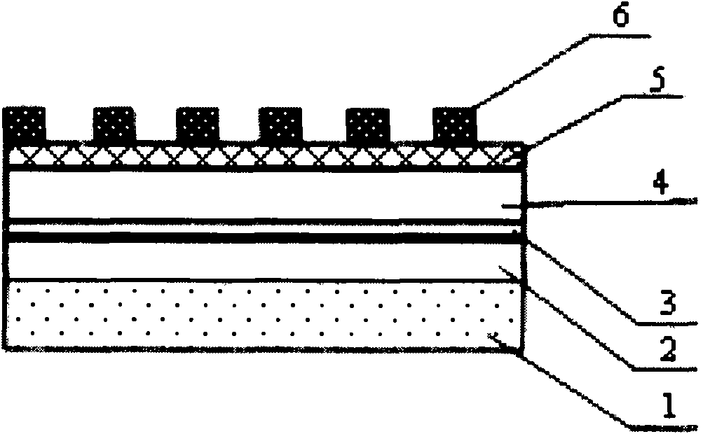
[0020] Embodiment one: see figure 1 , the present embodiment provides a light-emitting diode chip with a thin-film dielectric transition layer structure metal grating enhanced polarized light output, the structure includes: the LED emits light in the visible light range of 360-760 nanometers, the substrate 1 of the LED is GaN, and its refractive index is 2.5; n-type GaN layer 2; InGaN / GaN quantum well 3; p-type GaN layer 4; metal grating 6, the material of the metal grating can be Al, Ag, Au, Cu or their alloys, and the period of the metal grating ranges from 10 to 500 nanometers, the duty cycle is 0.1-0.9, the thickness of the grating is 10-300 nanometers; the dielectric transition layer 5 is a thin film structure, plated on the upper surface of the p-type GaN layer, and forms a composite structure with the metal grating (6), and the dielectric transition layer is MgF 2 (refractive index 1.38) or ZnS (refractive index 2.44), the refractive index is greater than 1.0, less than...

Embodiment 2

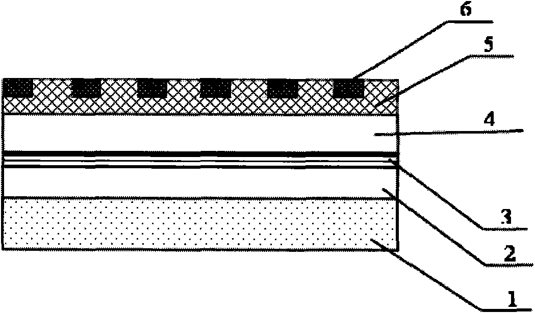
[0021] Embodiment two: see figure 2 , the present embodiment provides a metal grating-enhanced polarized light-emitting diode chip with an embedded dielectric transition layer structure. Ratio of 2.5, n-type GaN layer 2, InGaN / GaN quantum well 3, p-type GaN layer 4, metal grating 6, the metal grating material can be Al, Ag, Au, Cu or their alloys, the period range of the metal grating is 10 to 500 nanometers, the duty cycle is 0.1 to 0.9, and the thickness of the grating is 10 to 300 nanometers; the dielectric transition layer 5 is an embedded structure, plated on the upper surface of the p-type GaN layer, and forms a composite structure with the metal grating (6). Layer is MgF 2 (refractive index 1.38) or ZnS (refractive index 2.44), the refractive index is greater than 1.0, less than GaN's refractive index 2.5; in the embedded structure medium transition layer, the upper layer of the metal grating layer (6) and the p-type GaN layer (4) The surface interval is 10-100 nanom...

Embodiment 3

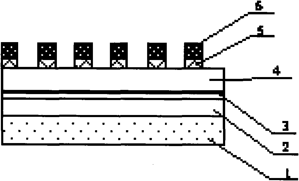
[0022] Embodiment three: see image 3, the embodiment of the present invention provides a metal grating enhanced polarized light-emitting diode chip with a dielectric transition layer grating structure, a substrate 1; an n-type GaN layer 2; an InGaN / GaN quantum well 3; a p-type GaN layer 4; a dielectric transition layer The grating 5; the metal grating 6; the material of the selected transition layer is MgF with a refractive index of 1.38 2 and ZnS with a refractive index of 2.44, the material of the metal grating is aluminum (Al), the thickness of the aluminum grating is 150 nanometers, and the duty ratio is 0.5. ZnS thickness 40nm, MgF 2 The thickness is 30 nanometers, and the duty ratio of the transition layer grating is consistent with that of the aluminum grating is 0.5.

[0023] see Figure 4 and Figure 5 : The comparison of the polarized light output characteristics in the grating period of 50-180 nanometers is given. In the curves of each legend, curve 1 is the c...


PUM

PropertyMeasurementUnit
Thicknessaaaaaaaaaa
Thicknessaaaaaaaaaa
Thicknessaaaaaaaaaa

Abstract

The invention relates to a light-emitting diode (LED) light source which produces light through a semiconductor band gap structure, in particular to an electromagnetic wave transmission structure, namely an active polarized light emission optical device with a composite micro-nano surface grating structure. The LED comprises a substrate (1), an n-type layer (2), a quantum well (3), a p-type layer (4) and a metal grating (6) and is characterized in that: a composite structure of a medium transition layer (5) and the metal grating (6) is plated or etched on the upper surface of the p-type layer (4); the refraction index of the medium transition layer meets the conditions that: n is greater than 1.0 and less than the refraction index of the p-type layer medium (4); and the transition layer is one of a thin film structure, a grating structure and an embedded structure. Due to the adoption of the structure, the transmission and extinction characteristics of the LED can be enhanced effectively; and in a period, the flatness of the side face of the grating, the duty ratio of the grating, and the range of working wavelengths are obviously improved compared with those of a conventional single-layer metal grating.

Description

technical field [0001] The invention relates to a light-emitting diode (LED) light source for generating light with a semiconductor bandgap structure, in particular to an electromagnetic wave transmission structure and an active polarized light-emitting optical device with a composite micro-nano surface grating structure. Background technique [0002] A light emitting diode (LED) is a semiconductor light source device that emits light in an electrically stimulated manner. The basic principle of LED light emission is: using a semiconductor chip with a pn junction structure, when a forward bias is applied, electrons and holes are injected from the n-type region and p-type region respectively, and the recombination of electrons and holes is released in the form of photons The energy and emission wavelength depend on the forbidden band width of the material. Currently, depending on the semiconductor material, LED light emission wavelengths cover the entire visible light wavelen...

Claims


Application Information

Patent Timeline
IPC IPC(8): H01L33/44
Inventor 张桂菊曹冰王钦华韩琴
Owner SUZHOU UNIV
Why Eureka
Try Eureka