Oxide-nitride-oxide stack containing a plurality of oxynitrides layers

A second oxynitride layer, oxynitride technology, applied in the direction of coating, gaseous chemical plating, metal material coating process, etc., can solve problems such as reverse effects, and achieve the effect of increasing speed

Active Publication Date: 2010-10-13
CYPRESS SEMICON CORP
View PDF4 Cites 32 Cited by
  • Summary
  • Abstract
  • Description
  • Claims
  • Application Information

AI Technical Summary

Problems solved by technology

Therefore, the charge storage characteristics of the memory 100 including the ONO stack 104, especially the programming and erasing speed and data retention, have the opposite effect.

Method used


Image

  • Oxide-nitride-oxide stack containing a plurality of oxynitrides layers
  • Oxide-nitride-oxide stack containing a plurality of oxynitrides layers
  • Oxide-nitride-oxide stack containing a plurality of oxynitrides layers

Examples


Embodiment Construction

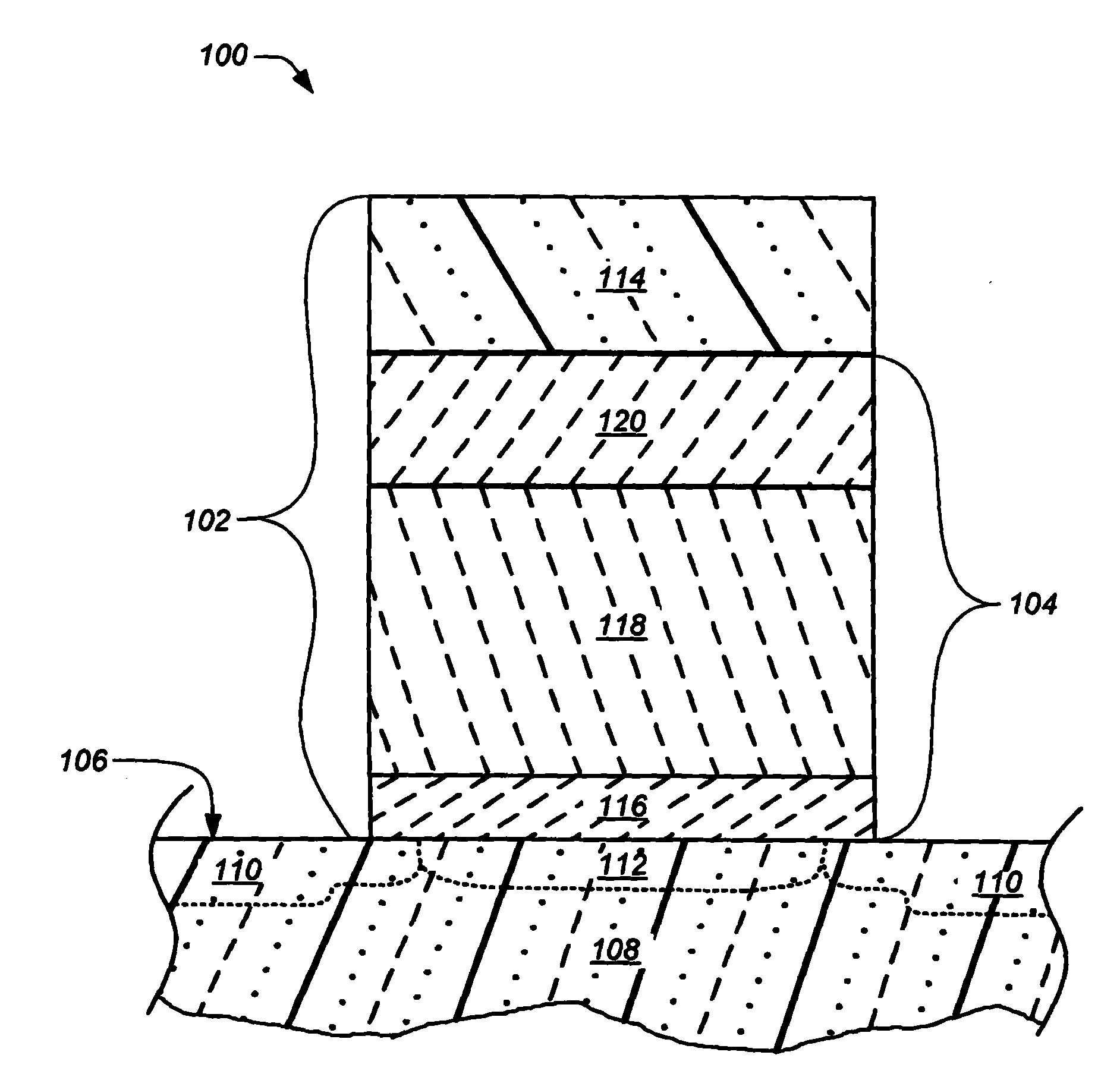
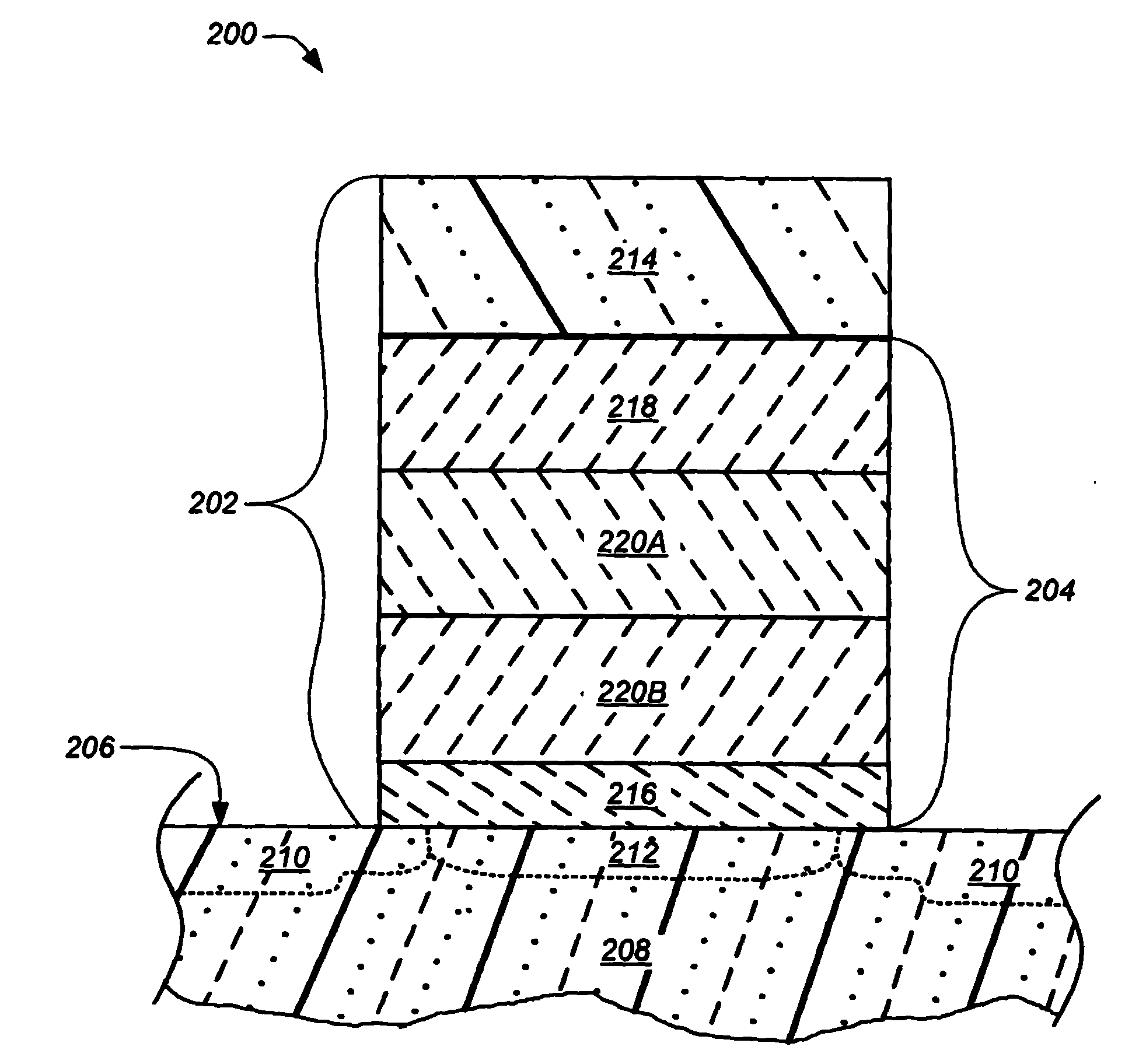
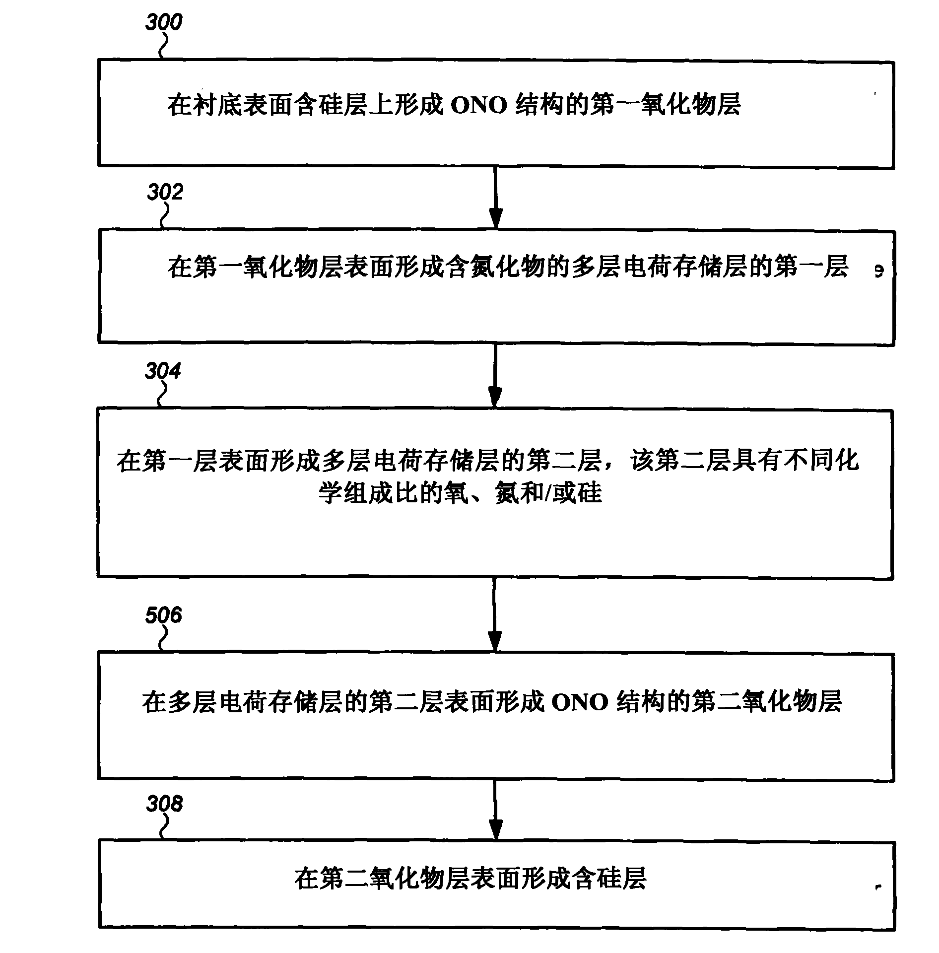
[0040] The present invention mainly discusses the Oxide-Nitride-Oxide (ONO) structure including multi-layer charge storage layer and its fabrication method. The ONO structure and its manufacturing method are especially suitable for forming storage layers of storage devices, such as silicon-oxide-nitride-oxide-silicon (SONOS) storage transistors.

[0041]In the ensuing description, numerous specific details are set forth in order to provide a thorough understanding of the present invention. The invention can be practiced by one skilled in the art without these specific details. In other instances, well-known structures and techniques have not been described in detail or shown in the drawings in order not to unnecessarily obscure the present invention.

[0042] Reference to "embodiments" in the description of the present invention means that specific functions, structures, materials, or features described in the relevant embodiments are included in at least one embodiment of th...


PUM


Abstract

The invention discloses a semiconductor device of an oxide-nitride-oxide (ONO) stack containing a plurality of charge storage layers and a forming method thereof. Generally, the method comprises the following steps of: firstly, forming a first oxide layer on an ONO structure; secondly, forming the plurality of charge storage layers containing nitride on the first oxide layer; and thirdly, forming a second oxide layer in the ONO structure on the plurality of charge storage layers. Preferably, each charge storage layer comprises at least two silicon oxynitride layers with two chemical constitutional ratios of oxygen, nitrogen and/or silicon. More preferably, the ONO structure is a part of a silicon-oxide-nitride-oxide-silicon (SONOS) structure, and the semiconductor device is an SONOS memory transistor.

Description

technical field [0001] The present invention relates to semiconductor manufacturing processes, and more particularly to oxide-nitride-oxide stacks containing improved nitrided oxide or oxynitride layers and methods of forming the same. Background technique [0002] Non-volatile semiconductor memories such as split-gate flash memory generally use stacked floating-gate field effect transistors. In this transistor, electrons are injected into the floating gate of the memory cell to be programmed by biasing the control gate to ground the body region of the substrate on which the memory cell is formed. [0003] An oxide-nitride-oxide (ONO) stack is used as the charge storage layer in silicon-oxide-nitride-oxide-silicon (SONOS) transistors, or as the floating gate in split-gate flash memory and the isolation layer between the control gate. [0004] figure 1 is a cross-sectional view of the intermediate structure of the semiconductor device 100 . Semiconductor device 100 includ...

Claims


Application Information

Patent Timeline
Patent Type & Authority Applications(China)
IPC IPC(8): H01L21/316C23C16/44H01L21/283H01L29/792H01L29/423
CPCH01L29/40114H01L21/285H10B41/30
Inventor 赛格·利维克里希纳斯瓦米·库马尔弗雷德里克·詹纳萨姆·吉哈
Owner CYPRESS SEMICON CORP
Why Eureka
Try Eureka