

Method for separating base plate and semiconductor layer
A semiconductor and substrate technology, applied in the field of separating the substrate and the semiconductor layer, can solve the problems of poor quality, high lattice mismatch, affecting the luminous efficiency, etc., to achieve increased luminous efficiency, simple manufacturing process steps and reduced technical costs Effect
- Summary
- Abstract
- Description
- Claims
- Application Information
AI Technical Summary
Problems solved by technology
Method used
Image

Examples
Embodiment Construction
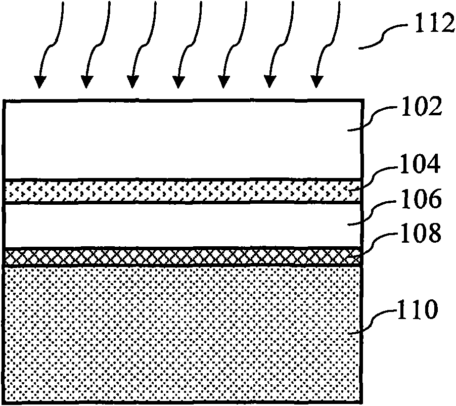
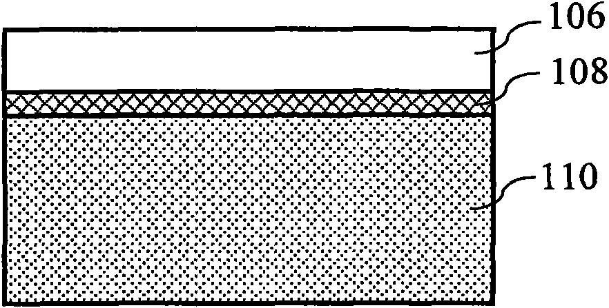
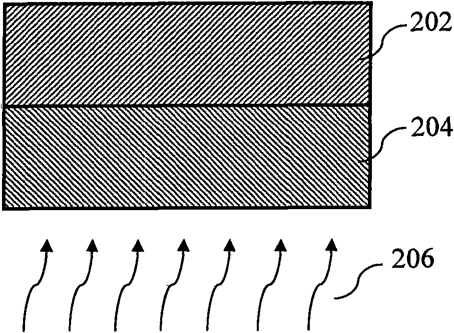
[0061] The subject matter of the present invention is a method for separating a substrate and a semiconductor layer. In order to provide a thorough understanding of the present invention, detailed steps and components thereof will be set forth in the following description. Obviously, the practice of the present invention is not limited to specific details well known to those of ordinary skill in the semiconductor optoelectronic fabrication process. On the other hand, well-known components or steps have not been described in detail so as not to unnecessarily limit the invention. The preferred embodiments of the present invention will be described in detail as follows, but in addition to these detailed descriptions, the present invention can also be widely implemented in other embodiments, and the scope of the present invention is not limited, it is based on the scope of the claims .
[0062] One object of the present invention is to separate the substrate and the semiconducto...
PUM
| Property | Measurement | Unit |
|---|---|---|
| Thickness | aaaaa | aaaaa |
| Groove width | aaaaa | aaaaa |
Abstract
Description
Claims
Application Information