Film transistor and manufacturing method of its lightly mixed drain area

A thin film transistor, lightly doped drain technology, applied in transistors, semiconductor/solid-state device manufacturing, electrical components, etc., can solve problems such as difficult mask pattern alignment, and achieve the effect of improving production efficiency and simplifying manufacturing process steps

Inactive Publication Date: 2006-04-12
CHUNGHWA PICTURE TUBES LTD
View PDF0 Cites 4 Cited by
  • Summary
  • Abstract
  • Description
  • Claims
  • Application Information

AI Technical Summary

Problems solved by technology

However, the above method of manufacturing the lightly doped drain region is likely to cause difficulties in the pattern alignment of the mask, and even through the self-aligned doping method, the complexity of the manufacturing process steps cannot be avoided.

Method used


Image

  • Film transistor and manufacturing method of its lightly mixed drain area
  • Film transistor and manufacturing method of its lightly mixed drain area
  • Film transistor and manufacturing method of its lightly mixed drain area

Examples


Embodiment Construction

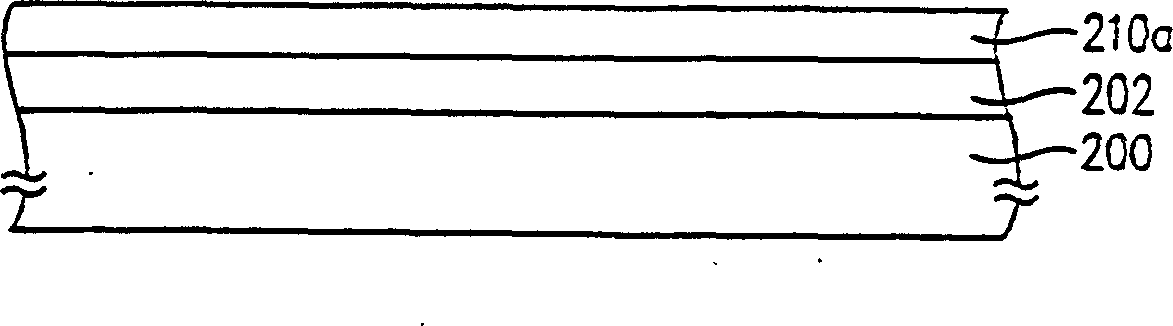
[0018] Please refer to Figure 2A~2I , Which sequentially show a schematic diagram of the manufacturing process of a thin film transistor of the present invention.

[0019] First of all, such as Figure 2A As shown, a buffer layer 202 is selectively formed on the substrate 200, and an amorphous silicon layer 210a is formed on the buffer layer 202. The material of the substrate 200 is, for example, glass, and the material of the buffer layer 202 is, for example, silicon dioxide. Its function is to enhance the substrate 200 and the subsequent polysilicon layer 210 (represented in Figure 2B ), and when the substrate 200 contains metal ions such as sodium, it can be used to prevent the metal ions in the substrate 200 from contaminating the polysilicon layer 210 (represented in Figure 2B ).

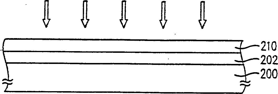
[0020] Then, like Figure 2B As shown, dehydrogenation treatment is performed and laser annealing treatment is performed on the amorphous silicon layer 210a, which is, for example, an excimer la...


PUM


Abstract

This invention relates to a method for manufacturing a light doped drain region of a film transistor, which first of all forms a polysilicon layer on the base plate then forms a grating insulation layer on the polysilicon layer, after that forms a buffer and a grating on the grating insulation layer, in which, the grating is set on the buffer and exposes part of the buffer, then carries out a doping manufacture technology and forms a light doped drain region in the polysilicon layer corresponding to the lower part of the buffer exposed by the grating.

Description

Technical field [0001] The present invention relates to a semiconductor device and a manufacturing method thereof, and more particularly to a method for manufacturing a thin film transistor and a lightly doped drain region thereof. Background technique [0002] Early polysilicon thin film transistors were manufactured using a solid phase crystallization (SPC) manufacturing process, but the manufacturing process temperature was as high as 1,000 degrees Celsius, so a quartz substrate with a higher melting point must be used. However, since the cost of the quartz substrate is much more expensive than that of the glass substrate, and due to the size of the substrate, the panel is only about 2 to 3 inches, so in the past, only small panels could be developed. In recent years, with the continuous advancement of laser technology, an Excimer Laser Annealing (ELA) manufacturing process has been developed, which uses a laser beam to irradiate the amorphous silicon film to melt the amorphou...

Claims


Application Information

Patent Timeline
Patent Type & Authority Applications(China)
IPC IPC(8): H01L29/786H01L21/336
Inventor 张锡明
Owner CHUNGHWA PICTURE TUBES LTD
Why Eureka
Try Eureka