Structure of wide gain spectrum quantum dot material for semiconductor optical amplifier
A technology of quantum dot materials and optical amplifiers, applied to the structure of the active region, etc., can solve the problems of speed bottleneck and high system cost
- Summary
- Abstract
- Description
- Claims
- Application Information
AI Technical Summary
Problems solved by technology
Method used
Image
Examples
Embodiment Construction
[0035] In order to make the object, technical solution and advantages of the present invention clearer, the present invention will be described in further detail below in conjunction with specific embodiments and with reference to the accompanying drawings.
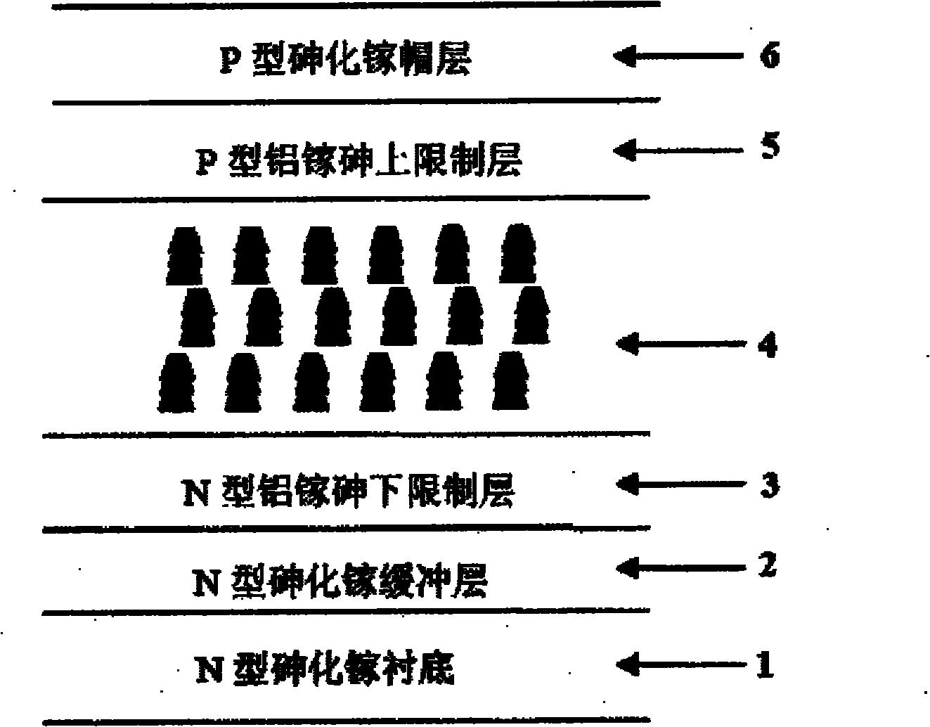
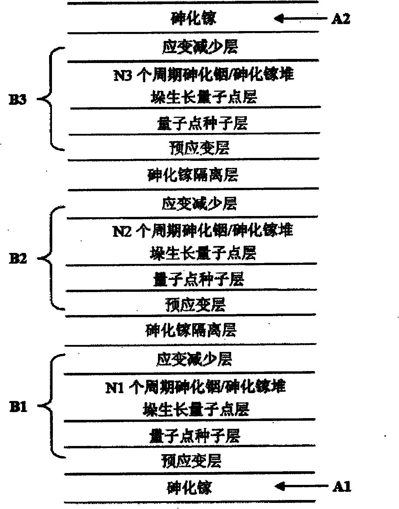
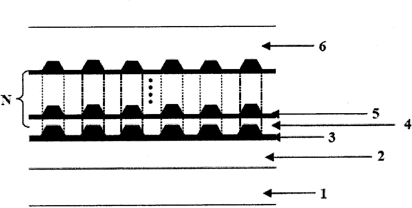
[0036] Please refer to the accompanying drawings, figure 1 It is a schematic diagram of a wide gain spectrum quantum dot material structure for a semiconductor optical amplifier provided by the present invention. The structure utilizes the non-uniform broadening characteristics of quantum dots designed with multiple layers of different sizes to obtain a wide gain spectrum, including:
[0037] An N-type gallium arsenide substrate 1;
[0038] An N-type gallium arsenide buffer layer 2, grown on the N-type gallium arsenide substrate 1 at a growth temperature of 600°C, for isolating defects on the substrate;
[0039] An N-type AlGaAs optical lower confinement layer 3, grown on the N-type GaAs buffer layer 2 at a growth temper...
PUM
| Property | Measurement | Unit |
|---|---|---|
| Thickness | aaaaa | aaaaa |
| Thickness | aaaaa | aaaaa |
Abstract
Description
Claims
Application Information


