Structure design of active region of a multi-wavelength gan-based vertical cavity surface emitting laser
A technology of vertical cavity surface emission and structure design, which is applied to the structure of the active region, the device for controlling the output parameters of the laser, the laser and other directions, which can solve the problems such as the difficulty in realizing the p-type ohmic contact and the difficulty in growing the nitride distributed Bragg mirror. , to achieve the effect of large gain and broad application prospects
- Summary
- Abstract
- Description
- Claims
- Application Information
AI Technical Summary
Problems solved by technology
Method used
Image
Examples
Embodiment 1
[0045] Embodiment 1: Multilayer stacked quantum dot active region structure design.
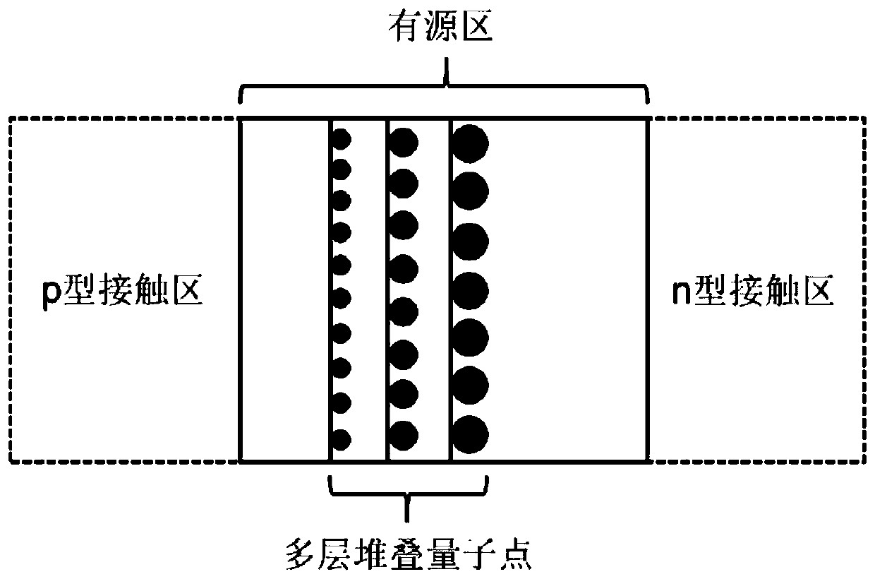
[0046] Such as figure 1 As shown, the multilayer stacked quantum dot active region is located between the n-type contact region and the p-type contact region, and is composed of quantum dots of different sizes; quantum dots of the same size can be one layer or more than two layers, the present invention figure 1 The active region shown consists of three groups of monolayer quantum dots of different sizes. Among them, the photon energy emitted by small quantum dots is large, that is, the emission wavelength is short; the photon energy emitted by large quantum dots is small, and the emission wavelength is long; the central wavelength of emission of quantum dots of different sizes must be consistent with the wavelength of the emitted laser.
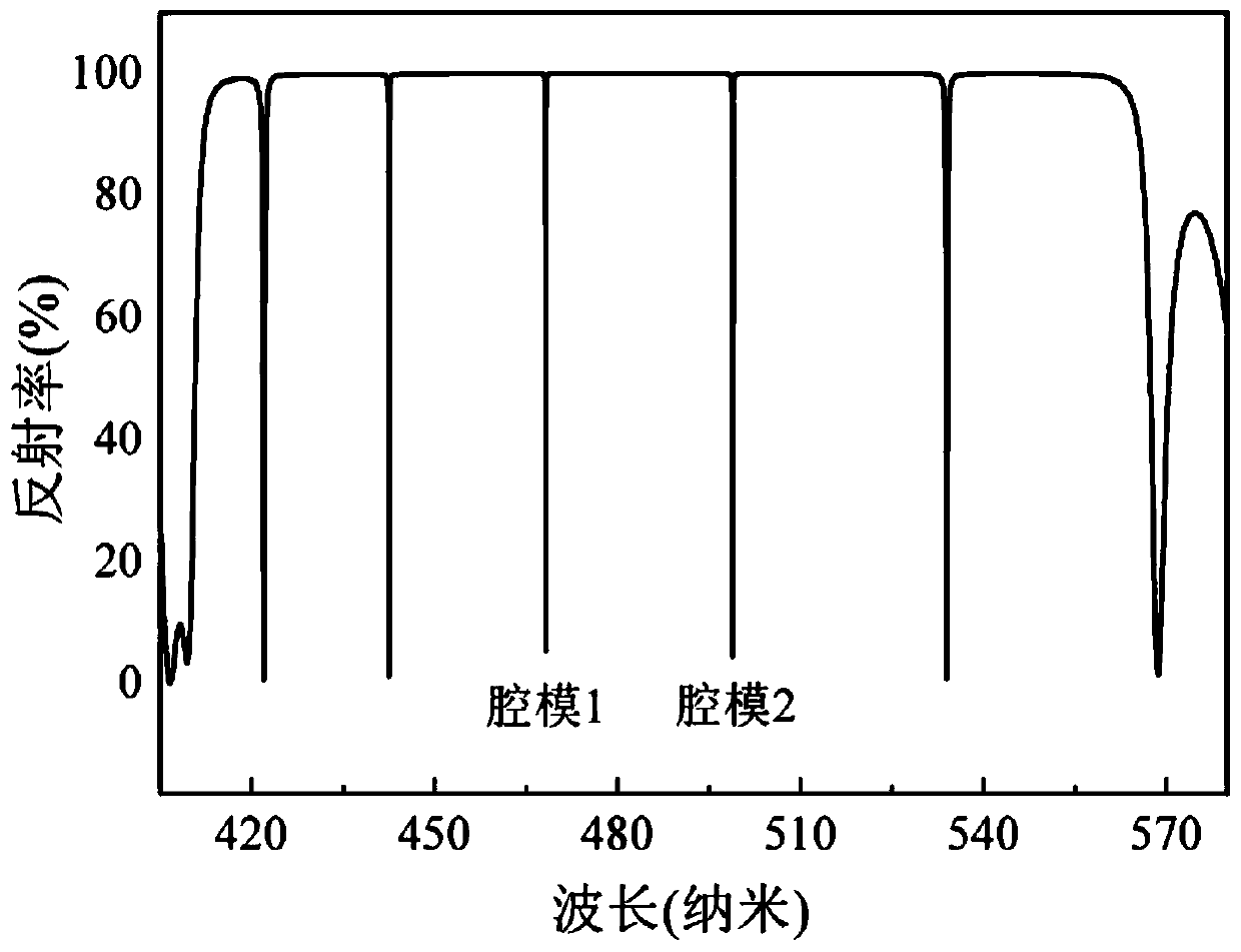
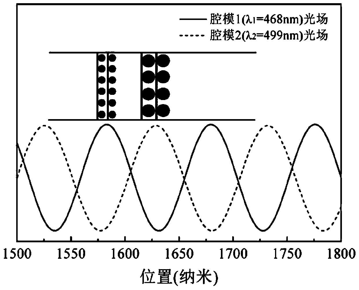
[0047] Assume that the wavelength of the laser to be emitted is λ 1 and lambda 2 . First, according to the laser wavelength λ 1 and lambda 2 Determin...
Embodiment 2
[0051] Embodiment 2: A multi-wavelength GaN-based vertical cavity surface emitting laser structure fabricated by using the multi-layer stacked quantum dot active region.
[0052] Such as Figure 4 As shown, the device structure is as follows:
[0053] Substrate, can adopt sapphire substrate, silicon carbide substrate, gallium nitride substrate and silicon substrate etc., the present invention selects sapphire substrate;
[0054] The bottom reflector can use nitride DBR or dielectric film DBR. Nitride DBR includes AlN / GaN DBR, AlGaN / GaN DBR, AlInN / GaN DBR and Al x Ga 1-x N / Al y Ga 1-y N DBR, etc., where x≠y; dielectric film DBR includes TiO 2 / SiO 2 DBR, ZrO 2 / SiO 2 DBR, Ta 2 o 5 / SiO 2 DBR, Si 3 N 4 / SiO 2 DBR and HfO 2 / SiO 2 DBR, etc., the present invention chooses AlN / GaN DBR as an example;
[0055] The n-type contact region is an n-type GaN layer doped with Si;
[0056] The n-type metal electrode is CrAu (20 / 200 nanometers);
[0057] The active region ...
PUM
| Property | Measurement | Unit |
|---|---|---|
| reflectance | aaaaa | aaaaa |
Abstract
Description
Claims
Application Information


