Method for doping grid electrode, drain electrode and source electrode in semiconductor manufacturing process

A process flow, semiconductor technology, applied in semiconductor/solid-state device manufacturing, semiconductor devices, electrical components, etc., can solve problems such as reducing device quality

Active Publication Date: 2010-11-10
SEMICONDUCTOR MANUFACTURING INTERNATIONAL (BEIJING) CORP
View PDF0 Cites 3 Cited by
  • Summary
  • Abstract
  • Description
  • Claims
  • Application Information

AI Technical Summary

Problems solved by technology

[0008] It can be seen that although the method in the prior art can achieve different concentrations of doping of the gate, drain, and source, it will produce a tunneling effect in which the drain and source are turned on, thereby reducing the quality of the device.

Method used


Image

  • Method for doping grid electrode, drain electrode and source electrode in semiconductor manufacturing process
  • Method for doping grid electrode, drain electrode and source electrode in semiconductor manufacturing process
  • Method for doping grid electrode, drain electrode and source electrode in semiconductor manufacturing process

Examples


Embodiment Construction

[0028] In order to make the object, technical solution and advantages of the present invention clearer, the present invention will be further described in detail below with reference to the accompanying drawings and examples.

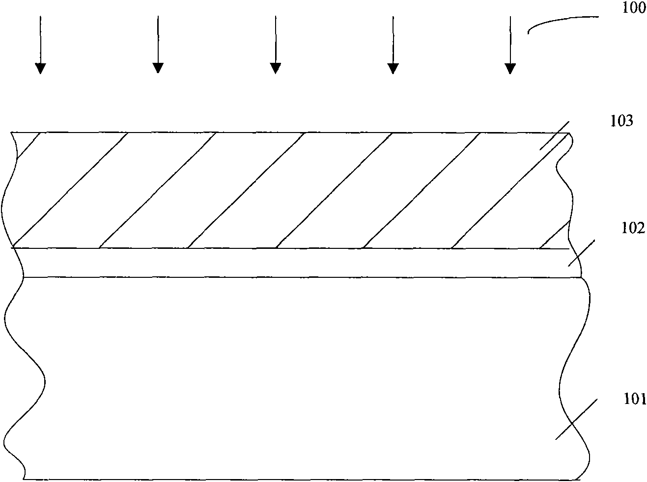
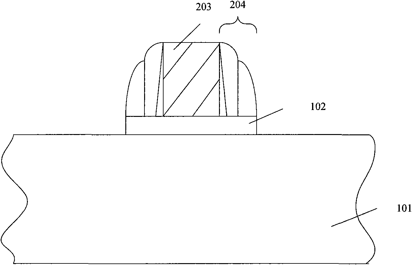
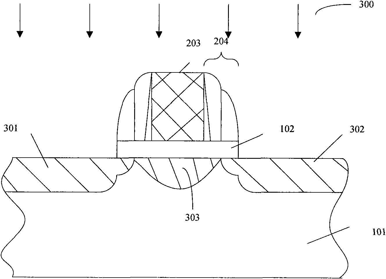
[0029] In order to make the doping concentration of the gate greater than the doping concentration of the drain and the source, the present invention still performs two ion implantations, but blocks the ion implantation to the substrates on both sides of the gate during the first ion implantation process, so that the ions It can only be implanted into the gate, and then ensure that the ions can be implanted into the gate and the substrate on both sides of the gate to form the source and drain during the second ion implantation. In this way, since the gate is doped by ion implantation twice, and the source and drain are doped by ion implantation only once respectively, it can be ensured that the doping concentration of the gate is greater than that of the...


PUM


Abstract

The invention discloses a method for doping a grid electrode, a drain electrode and a source electrode in the semiconductor manufacturing process. The method comprises the following steps of: forming the grid electrode on a substrate, then coating bottom anti-reflective coating (BARC) on the surface of the grid electrode and the surfaces of the substrates at two sides of the grid electrode, wherein the BARC coated on the surface of the substrate is higher than the surface of the grid electrode; etching the BARC which is higher than the surface of the grid electrode, enabling the BARC on the surfaces of the substrates at two sides of the grid electrode to the surface of the grid electrode, and carrying out first ion implantation; eliminating the BARC; and carrying out ion implantation again. The method can realize the doping with the grid electrode, the drain electrode and the source electrode in different concentrations and prevent the tunneling effect.

Description

technical field [0001] The invention relates to the field of semiconductor manufacturing, in particular to a method for doping gates, drains, and sources in the semiconductor manufacturing process flow. Background technique [0002] With the wide application of electronic equipment, the manufacturing process of semiconductors has been developed rapidly. In the manufacturing process of semiconductors, doping processes are involved. Specifically, polysilicon is doped by ion implantation to form gates, and The substrate on both sides of the gate is doped to form the drain and source. [0003] However, according to actual needs, the doping concentration of the gate is generally required to be greater than the doping concentration of the drain and the source. Therefore, the doping method for achieving different doping concentrations in the prior art includes the following steps: [0004] Step one, see figure 1 A gate oxide layer 102 and a polysilicon layer 103 are formed on a s...

Claims


Application Information

Patent Timeline
Patent Type & Authority Applications(China)
IPC IPC(8): H01L21/28H01L21/312H01L21/311H01L21/265H01L21/336
Inventor 吴永玉何学缅陈海华刘思南
Owner SEMICONDUCTOR MANUFACTURING INTERNATIONAL (BEIJING) CORP
Why Eureka
Try Eureka