Film transistor array substrate and manufacturing method thereof

A technology of thin film transistors and array substrates, which is applied in the field of metal layer formation of thin film transistor array substrates, and can solve problems such as low resistivity, hillock growth, and increased resistance of scanning lines and data lines.

Active Publication Date: 2010-11-17
CENTURY DISPLAY (SHENZHEN) CO LTD
View PDF6 Cites 11 Cited by
  • Summary
  • Abstract
  • Description
  • Claims
  • Application Information

AI Technical Summary

Problems solved by technology

[0004] In the above-mentioned pixel structure, the gate has a double-layer structure of molybdenum (Mo) metal layer and aluminum neodymium (AlNd) layer, although aluminum neodymium (AlNd) has better temperature stability than aluminum (Al) metal, It can prevent the problem of hillock growth caused by excessive extrusion stress between aluminum atomic grains during high temperature film formation, but aluminum neodymium (AlNd) has a higher resistivity than aluminum (Al) metal Shortcomings
[0005] Considering the increasing trend of LCD size, however, the length of scan lines and data lines will increase with the increase of LCD size, so that the increasing scan lines and data lines will increase the resistance value

Method used


Image

  • Film transistor array substrate and manufacturing method thereof
  • Film transistor array substrate and manufacturing method thereof
  • Film transistor array substrate and manufacturing method thereof

Examples


Embodiment Construction

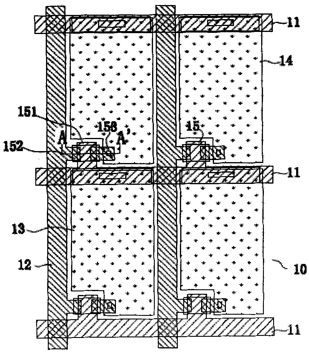
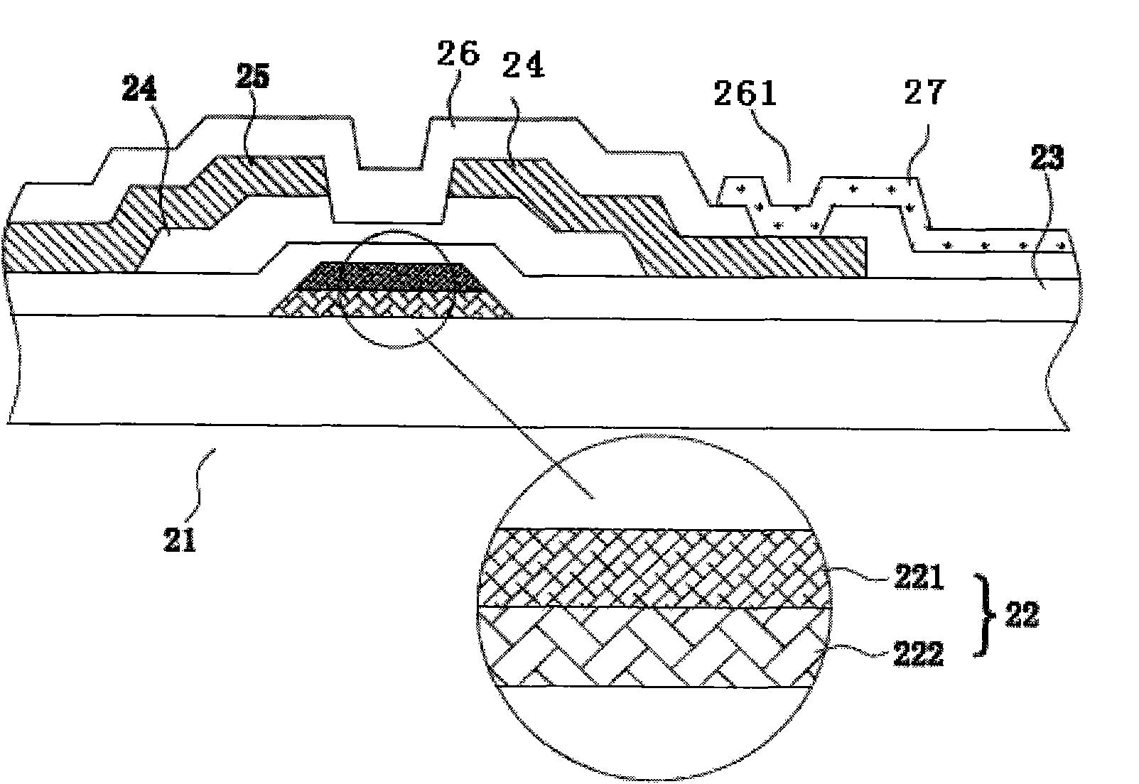
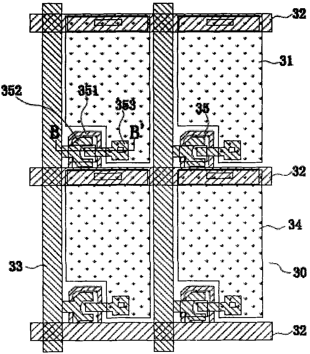
[0029] Preferred embodiments of the invention will be described more fully hereinafter with reference to the accompanying drawings, in which preferred embodiments of the invention are shown. However, this invention may also be embodied in different forms and should not be construed as limited to only the embodiments set forth herein. Rather, these embodiments are provided so that this disclosure will be thorough and complete, and will fully convey the scope of the invention to those skilled in the art.

[0030]In the drawings, the thickness of layers, films and regions are shown exaggerated for clarity. Like reference numerals refer to like elements throughout the drawings. It will also be understood that when an element such as a layer, film, region, or substrate is referred to as being "on" another element, it can be directly on the other element or intervening elements may be present.

[0031] Hereinafter, a thin film transistor array substrate and a manufacturing method ...


PUM


Abstract

The invention provides a film transistor array substrate and a manufacturing method thereof. The film transistor array substrate comprises a substrate, as well as a first metal layer, an insulating layer, a semiconductor layer, a second layer, a passivation layer and a transparent electrode layer which are formed on the substrate in turn, wherein the first metal layer at least comprises three layers of aluminum films, the second metal layer also consists of three aluminum films, and the three aluminum films have different film quality densities and are formed under different coating film parameters. Therefore, the film transistor array substrate provided with the at least three aluminum films not only has the characteristic of low resistivity, but also can prevent aluminum metal from generating hillock growth in the high-temperature film coating process.

Description

technical field [0001] The invention relates to a liquid crystal display thin film transistor array substrate and a manufacturing method of the array substrate; in particular, it relates to a method for forming a metal layer of the thin film transistor array substrate. Background technique [0002] At present, the use of liquid crystal displays (LCDs) has become a trend. LCDs have superior characteristics such as high image quality, better space utilization, low power consumption, and no radiation. With the increasingly mature technology of LCDs, LCDs Widely used in various fields. Generally speaking, a liquid crystal display is composed of a thin film transistor array substrate, a color filter substrate and a liquid crystal layer sandwiched between the two substrates. Wherein, the thin film transistor array substrate mainly includes a substrate and pixel structures arranged on the substrate in an array. The aforementioned pixel structure is mainly composed of scan lines, ...

Claims


Application Information

Patent Timeline
IPC IPC(8): H01L27/02H01L23/532H01L21/77H01L21/768G02F1/1362G02F1/1368
Inventor 黄展宽黄荣士王宣丽张晓星高翔李金磊
Owner CENTURY DISPLAY (SHENZHEN) CO LTD
Why Eureka
Try Eureka