Storage device and information re-recording method

A technology for storage devices and storage elements, which is applied in the field of storage devices and re-recording information, can solve the problems of large write current and difficulty in miniaturization, and achieve the effects of reducing the number of cycles, reducing time, and improving adjustment capabilities

Inactive Publication Date: 2010-11-17
SONY CORP
View PDF1 Cites 9 Cited by
  • Summary
  • Abstract
  • Description
  • Claims
  • Application Information

AI Technical Summary

Problems solved by technology

However, there is a problem that it is not easy to miniaturize in FeRAM, and there is a problem in that writing current is large in MRAM (for example, non-patent document 1)

Method used


Image

  • Storage device and information re-recording method
  • Storage device and information re-recording method
  • Storage device and information re-recording method

Examples


no. 1 approach

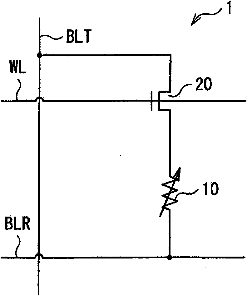
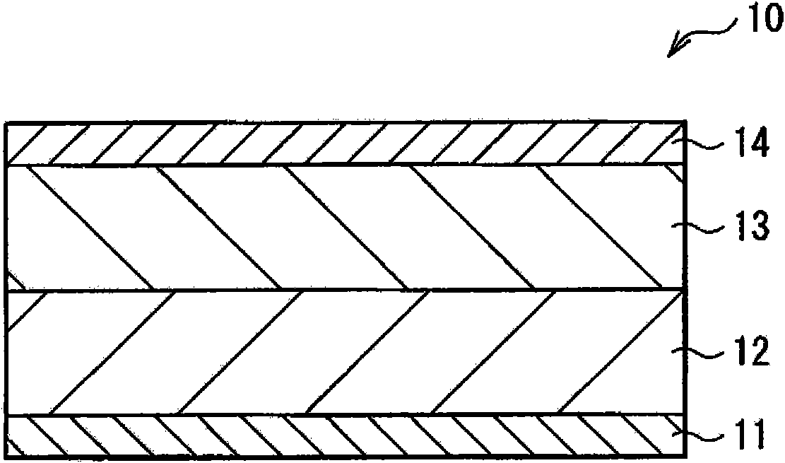
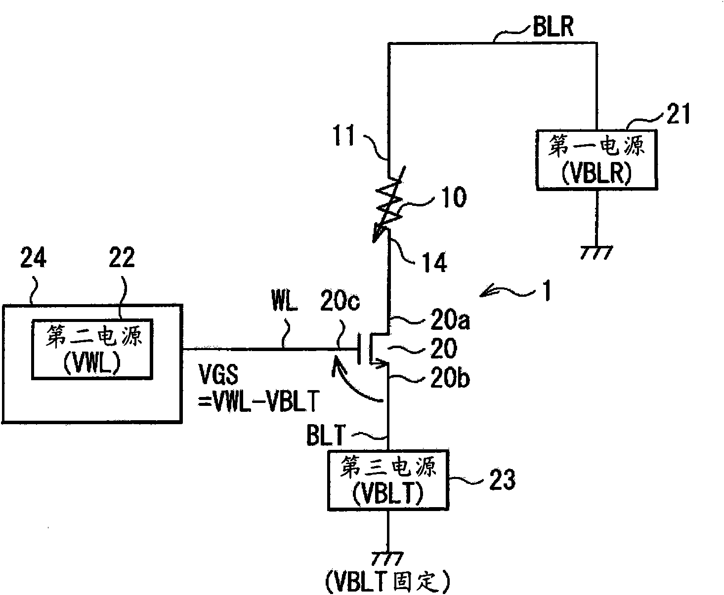
[0036] figure 1 Shows a storage unit L of the storage device according to the first embodiment of the present invention. The storage unit 1 includes: a memory element, for example, figure 2 The variable resistance element 10 shown in ; and the N-channel MOS type transistor 20 as a switching element. In this memory device, a plurality of memory cells 1 are arranged in an array state or a matrix state by regarding the memory cells 1 as memory units. image 3 An equivalent circuit at the time of a write operation of the memory cell 1 is shown.

[0037] For example, variable resistance element 10 is formed by stacking electrode 11 , ion source layer 12 , high resistance layer (variable resistance layer) 13 , and electrode 14 .

[0038] The electrodes 11 and 14 are composed of metal materials such as Al, Cu, and W, for example. The high-resistance layer 13 is formed of, for example, a metal material, a rare earth element, an oxide or nitride of a mixture of a metal material an...


PUM


Abstract

Provided is a storage device which can reduce the number of cycles required for a verify process upon a multi-value recording. The initial value of the potential difference VGS between a gate and a source of a switching transistor upon a verify process is varied in accordance with the resistance value level of the multi-value information. When the write side performs a 3-value recording, if '01' is the information, the initial value VGS01 is set to be smaller than VGS = 1.7V corresponding to the target resistance value level '01', and if '00' is the information, a value is set to be lower than VGS = 2.2 V corresponding to the target resistance value level '00' and higher than the aforementioned VGS01. This can reduce the number of cycles required for the verify process.

Description

technical field [0001] The present invention relates to a memory device including a memory cell having a memory element and a switching element and a method of rerecording information, and more particularly, to a memory device that performs rerecording by parity control. Background technique [0002] In information devices such as computers, high-density DRAM (Dynamic Random Access Memory) capable of high-speed operation has been widely used. However, in DRAM, there is a problem of high manufacturing cost due to complicated manufacturing process compared with logic circuits and signal processing circuits generally used in electronic devices. In addition, DRAM is volatile memory (the information in it is erased by turning off the power), and requires frequent refresh operations. [0003] Thus, as a nonvolatile memory in which information is not erased even if the power is turned off, for example, FeRAM (Ferroelectric Random Access Memory), MRAM (Magnetoresistive Random Acces...

Claims


Application Information

Patent Timeline
Patent Type & Authority Applications(China)
IPC IPC(8): G11C13/00
CPCG11C13/0069G11C13/0064G11C2213/79G11C2213/11G11C11/56G11C2013/0071G11C13/0011G11C2013/0092G11C2213/56
Inventor 对马朋人椎本恒则保田周一郎
Owner SONY CORP
Why Eureka
Try Eureka