Method for growing group III nitride nanometer material

A growth method and nanomaterial technology, applied in the field of growth and preparation of III-nitride nano-arrays, can solve problems that are not conducive to large-scale device production, contamination of reaction chambers, etc.

Inactive Publication Date: 2010-12-01
INST OF SEMICONDUCTORS - CHINESE ACAD OF SCI
View PDF0 Cites 32 Cited by
  • Summary
  • Abstract
  • Description
  • Claims
  • Application Information

AI Technical Summary

Problems solved by technology

This is not conducive to mass production of devices
Moreover, the introduction of metals can easily cause contamination of the reaction chamber.

Method used


Image

  • Method for growing group III nitride nanometer material
  • Method for growing group III nitride nanometer material
  • Method for growing group III nitride nanometer material

Examples


Embodiment Construction

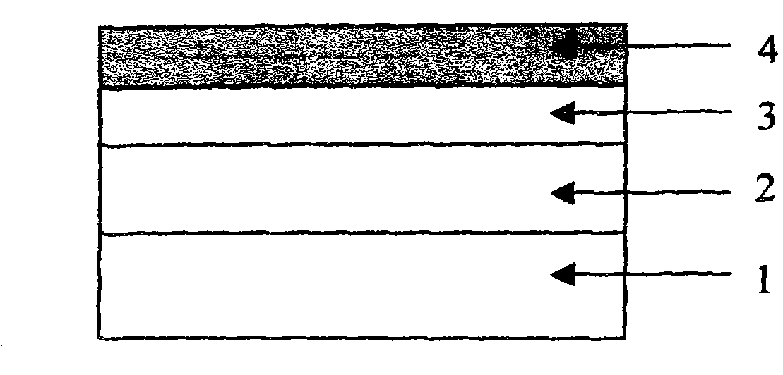
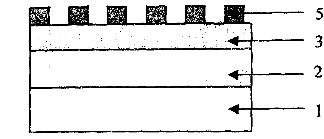
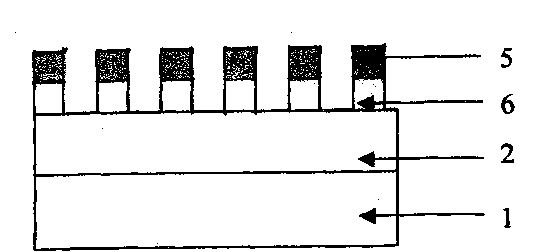
[0029] For the method that usually obtains nanowires or nanopillars, that is, the VLS growth method of metal catalysts, the obtained nanowires or nanopillars are usually randomly distributed on the substrate, and the direction of the nanowires or nanopillars is mostly not vertical. on the substrate. The nanowires need to be peeled off from the substrate to fabricate devices from a single nanocolumn. This is not conducive to mass production of devices. For the MOCVD system, the introduction of other metals outside the reaction system is likely to cause contamination of the reaction chamber. Therefore, a size-controllable and ordered capping layer of (gallium) indium nitride (In(Ga)N) perpendicular to the substrate is grown on GaN nanopillars by MOCVD system to form In(Ga)N / GaN nanopillars. Heterojunction array is a direction worthy of research. The method for growing III-group nitride nanometer materials provided by the invention does not use metal as a catalyst, and for MOC...


PUM


Abstract

The invention relates to a method for growing a group III nitride nanometer material, which comprises the following steps of: (1) epitaxially growing a GaN template, a SiO2 layer and a Ni metal film on a substrate in sequence; (2) enabling the Ni metal film to form self-organized nanometer Ni particles by using a two-step rapid thermal annealing method; (3) and etching the SiO2 layer by a dry method by using the self-organized nanometer Ni particles as a mask to form a SiO2 nanometer column; (4) etching the GaN template by the dry method by using the self-organized nanometer Ni particles and the SiO2 nanometer column formed by etching as masks to form GaN nanometer column array; (5) removing the SiO2 nanometer column and the nanometer Ni particles by using a BOE solution to obtain the GaN nanometer column array; and (6) growing the InN or InGaN group III nitride semiconductor material on the GaN nanometer column array, the side wall thereof and the bottom of the nanometer column array.

Description

technical field [0001] The invention relates to a growth method for growing group III nitride nanometer materials on gallium nitride (GaN) nanometer arrays produced by dry etching. Aim to grow high-quality, high-aspect-ratio III-nitride nanoarrays to form nanoarrays with structures such as core / shell radial heterojunctions, p-n junctions, and multiple quantum wells (MQW), which belong to III The field of growth and preparation of group nitride nano-arrays. Background technique [0002] Group III nitride nanostructures can introduce quantum confinement effects, improve stress relaxation states, and increase optical extraction efficiency, etc., and have received extensive attention in the past few years. For example, nitride nanostructures can increase the luminous intensity of nitride LEDs. [0003] At present, the growth methods of nanostructures are as follows: (1) Catalyst-assisted vapor-liquid-solid (VLS) growth: before growth, 2-10nm thick Ni, Fe, Au and other metals a...

Claims


Application Information

Patent Timeline
Patent Type & Authority Applications(China)
IPC IPC(8): C01B21/00C01B21/06C01B21/064B82B3/00
Inventor 孙苋刘文宝朱建军江德生王辉张书明刘宗顺杨辉
Owner INST OF SEMICONDUCTORS - CHINESE ACAD OF SCI
Why Eureka
Try Eureka