Integrated circuit structure

A technology of integrated circuit and fin structure, applied in the field of integrated circuit structure, can solve the problems of high source/drain resistance, low energy state density of conduction band, etc.

Active Publication Date: 2010-12-08
TAIWAN SEMICON MFG CO LTD
View PDF8 Cites 28 Cited by
  • Summary
  • Abstract
  • Description
  • Claims
  • Application Information

AI Technical Summary

Problems solved by technology

In addition, the low energy density of states in the conduction band leads to high source / drain resistance, which avoids the improvement of the final transistor drive current

Method used


Image

  • Integrated circuit structure
  • Integrated circuit structure
  • Integrated circuit structure

Examples


Embodiment Construction

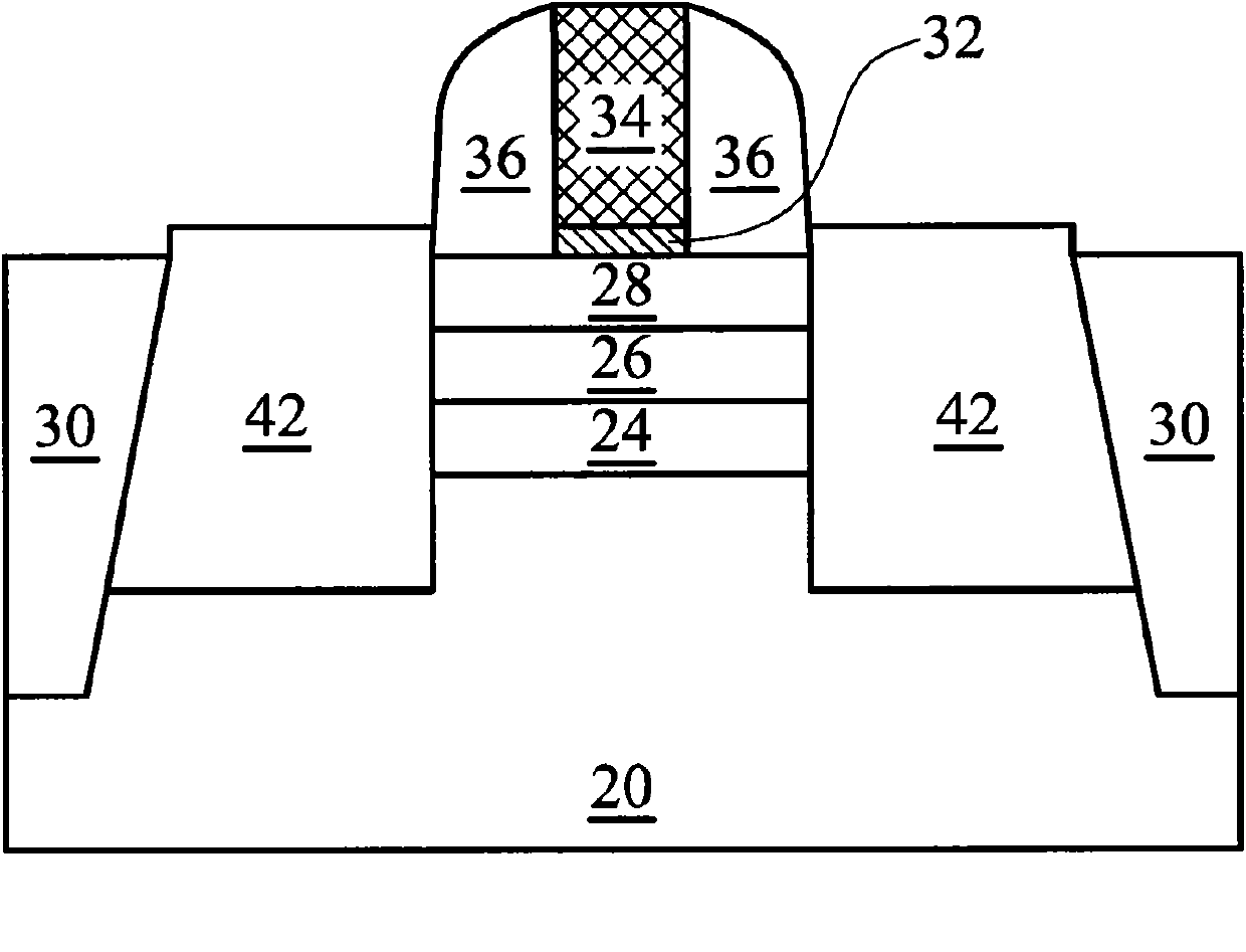
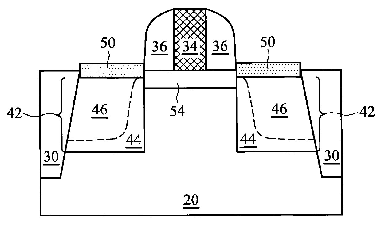
[0043] In the following, each embodiment is described in detail and examples accompanied by drawings are used as a reference basis of the present invention. In the drawings or descriptions in the specification, the same figure numbers are used for similar or identical parts. And in the drawings, the shape or thickness of the embodiments may be enlarged, and marked for simplicity or convenience. Furthermore, the parts of the components in the drawings will be described separately. It should be noted that the components not shown or described in the drawings are forms known to those skilled in the art. In addition, specific The examples are only for revealing specific methods used in the present invention, and are not intended to limit the present invention.

[0044] Embodiments of the present invention provide novel transistors including compound semiconductor materials composed of Group III and Group V elements (commonly referred to as III-V compound semiconductors), and a ma...


PUM


Abstract

An integrated circuit structure includes a substrate, and a channel over the substrate. The channel includes a first III-V compound semiconductor material formed of group III and group V elements. A gate structure is over the channel. A source/drain region is adjacent the channel and includes a group-IV region formed of a doped group-IV semiconductor material selected from the group consisting essentially of silicon, germanium, and combinations thereof. By re-growing silicon/germanium source/drain regions, the existing silicidation technique can be used to reduce the source/drain resistance and to improve drive currents of the resulting transistors. Buffer layers have the effect of smoothening the lattice constant transition between the channel of the transistor and the source/drain regions, resulting in a reduced defect density and reduced junction leakage currents.

Description

technical field [0001] The present invention relates to integrated circuit structures, and more particularly to transistors comprising III-V compound semiconductors and methods of manufacturing the same. Background technique [0002] There is a close correlation between the speed of a metal-oxide-semiconductor (MOS) transistor and the driving current of the MOS transistor, and the driving current of the MOS transistor is closely related to the mobility of charges. For example, when the electron mobility is high in the channel region, the NMOS transistor has a high driving current, whereas when the hole mobility is high in the channel region, the PMOS transistor has a high driving current. [0003] Compound semiconductor materials composed of Group III and Group V elements (commonly known as III-V compound semiconductors) are good candidates for forming NMOS transistors because of their high electron mobility. Therefore, III-V compound semiconductors are often used to form N...

Claims


Application Information

Patent Timeline
Patent Type & Authority Applications(China)
IPC IPC(8): H01L27/088H01L29/78H01L29/06H01L21/336
Inventor 柯志欣万幸仁
Owner TAIWAN SEMICON MFG CO LTD
Why Eureka
Try Eureka