Region-based photoelectric double-layer network-on-a-chip and routing method

A double-layer on-chip network and area technology, applied in electromagnetic wave transmission systems, transmission systems, digital transmission systems, etc., can solve problems affecting network performance, increasing implementation costs, and low wavelength utilization, so as to improve network performance and reduce congestion , Improve the effect of transmission speed and throughput

Inactive Publication Date: 2010-12-15
陕西光电子先导院科技有限公司
View PDF2 Cites 29 Cited by
  • Summary
  • Abstract
  • Description
  • Claims
  • Application Information

AI Technical Summary

Problems solved by technology

At present, some of the existing on-chip optical routers are blocked, which affects the network performance; some use multiple wavel

Method used


Image

  • Region-based photoelectric double-layer network-on-a-chip and routing method
  • Region-based photoelectric double-layer network-on-a-chip and routing method
  • Region-based photoelectric double-layer network-on-a-chip and routing method

Examples


Embodiment Construction

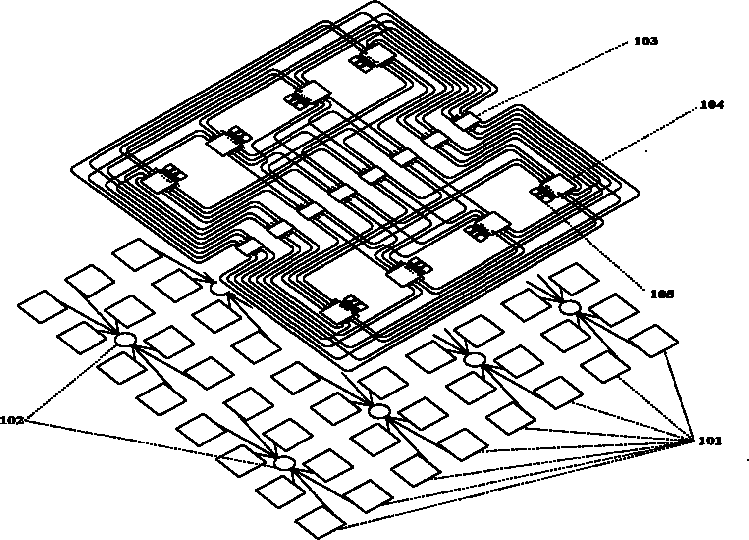
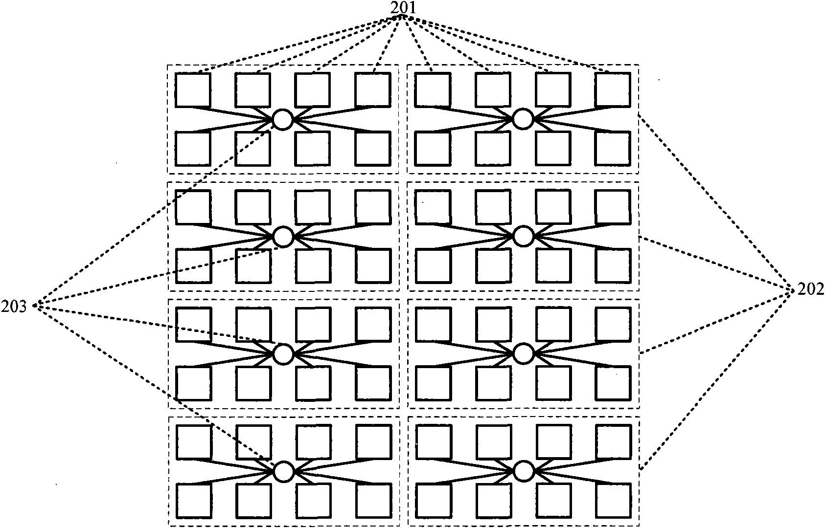
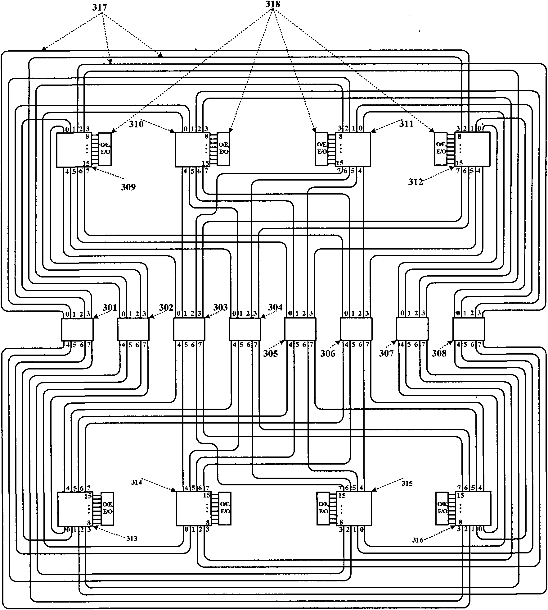
[0040] refer to figure 1 , the present invention discloses an area-based photoelectric double-layer on-chip network system, including: 64 processor cores 101, 8 electrical crossover matrix modules 102, 8 8-port optical routers 103 and 8 16-port optical routers 104. Considering the local characteristics of on-chip communication, the 64 processor cores are divided into 8 areas, and within each area, the 8 processor cores are interconnected by an electrical cross matrix module; between areas, the electrical The cross matrix module, 8-port optical router and 16-port optical router are divided into 3 levels, and each area is connected into a whole network according to the following rules:

[0041] Level 1, including 8 electrical cross matrix modules, each electrical cross matrix module has 16 ports, of which 8 ports are respectively connected to 8 processor cores, and the other 8 ports are respectively connected to the next 16 The 8 ports of the port optical router are connected o...


PUM


Abstract

The invention discloses a region-based photoelectric double-layer network-on-a-chip and a routing method for solving the problem of serious network congestion of the traditional network. The system comprises 64 processor cores, 8 electrical crossing matrix modules, 8 8-port optical routers and 8 16-port optical routers; the 64 processor cores are divided into 8 regions; in each region, one electrical crossing matrix module mutually connect the 8 processor cores uniformly; and among the regions, the electrical crossing matrix modules, the 8-port optical routers and the 16-port optical routers connects all the regions into an integrated network. When two communication parties are in the same region, data information can be exchanged directly through the electrical crossing matrix modules; and when the two communication parties are not in different regions, the data information can be exchanged among regions through the electrical crossing matrix modules, the 8-port optical routers and the 16-port optical routers. The invention can improve the resource utilization rate and can be used for the interconnection among cores on a chip and optimizing data transmission among the processor cores.

Description

technical field [0001] The invention belongs to the technical field of on-chip communication and relates to a network system, in particular to an area-based photoelectric double-layer on-chip network system, which can be used for interconnection between on-chip cores and optimizes data transmission between processor cores. Background technique [0002] With the rapid development of semiconductor technology, a single chip can integrate more and more complex functions. The scale of the system chip (System on Chip, SoC) is getting bigger and bigger, and it is developing towards the direction of multi-core and heterogeneous. As a new design method, Network on Chip (NoC) can solve the bottlenecks of energy consumption, area, and bandwidth caused by the bus-based structure, and meet the requirements of scalability, energy consumption, and area for the development of large-scale integrated circuits. , reusability, quality of service and other requirements, it not only has good sca...

Claims


Application Information

Patent Timeline
IPC IPC(8): H04L12/56H04L12/04H04B10/12H04L12/701
Inventor 顾华玺张晶杨银堂王军辉
Owner 陕西光电子先导院科技有限公司
Why Eureka
Try Eureka