Semiconductor device and method for manufacturing the same

A semiconductor and thin film transistor technology, applied in semiconductor/solid-state device manufacturing, semiconductor devices, transistors, etc., can solve the problems of complex manufacturing process, off-current suppression, etc., to simplify the manufacturing process, low off-leakage current, and turn-on Features and Disconnect Features Excellent effect

Inactive Publication Date: 2010-12-22
SHARP KK
View PDF5 Cites 4 Cited by
  • Summary
  • Abstract
  • Description
  • Claims
  • Application Information

AI Technical Summary

Problems solved by technology

[0009] As such, in the existing TFT structure, it is difficult to suppress the off current to a low level while increasing the on current, and it is necessary to select an optimal TFT structure according to the use and purpose of the TFT
Therefore, if a drive circuit-integrated active matrix substrate is to be produced, it is necessary to form TFTs for pixels and TFTs for drive circuits having mutually different structures on the same substrate, and there is a problem that the manufacturing process becomes complicated.

Method used


Image

  • Semiconductor device and method for manufacturing the same
  • Semiconductor device and method for manufacturing the same
  • Semiconductor device and method for manufacturing the same

Examples


no. 1 approach

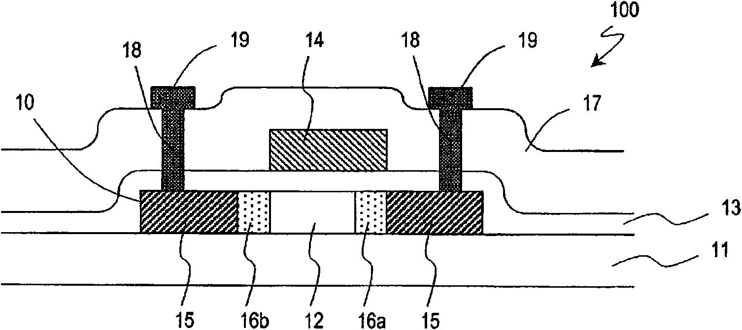
[0056] Hereinafter, a semiconductor device according to a first embodiment of the present invention will be described with reference to the drawings. The semiconductor device of this embodiment includes a thin film transistor described below.

[0057] figure 1 is a schematic cross-sectional view of a thin film transistor in this embodiment mode. The thin film transistor 100 has a semiconductor layer 10 supported by a substrate 11 having an insulating surface, a gate electrode 14 provided on the semiconductor layer 10 via a gate insulating film 13, an interlayer insulating film 17 covering the gate electrode 14, a source electrode / drain electrode 19.

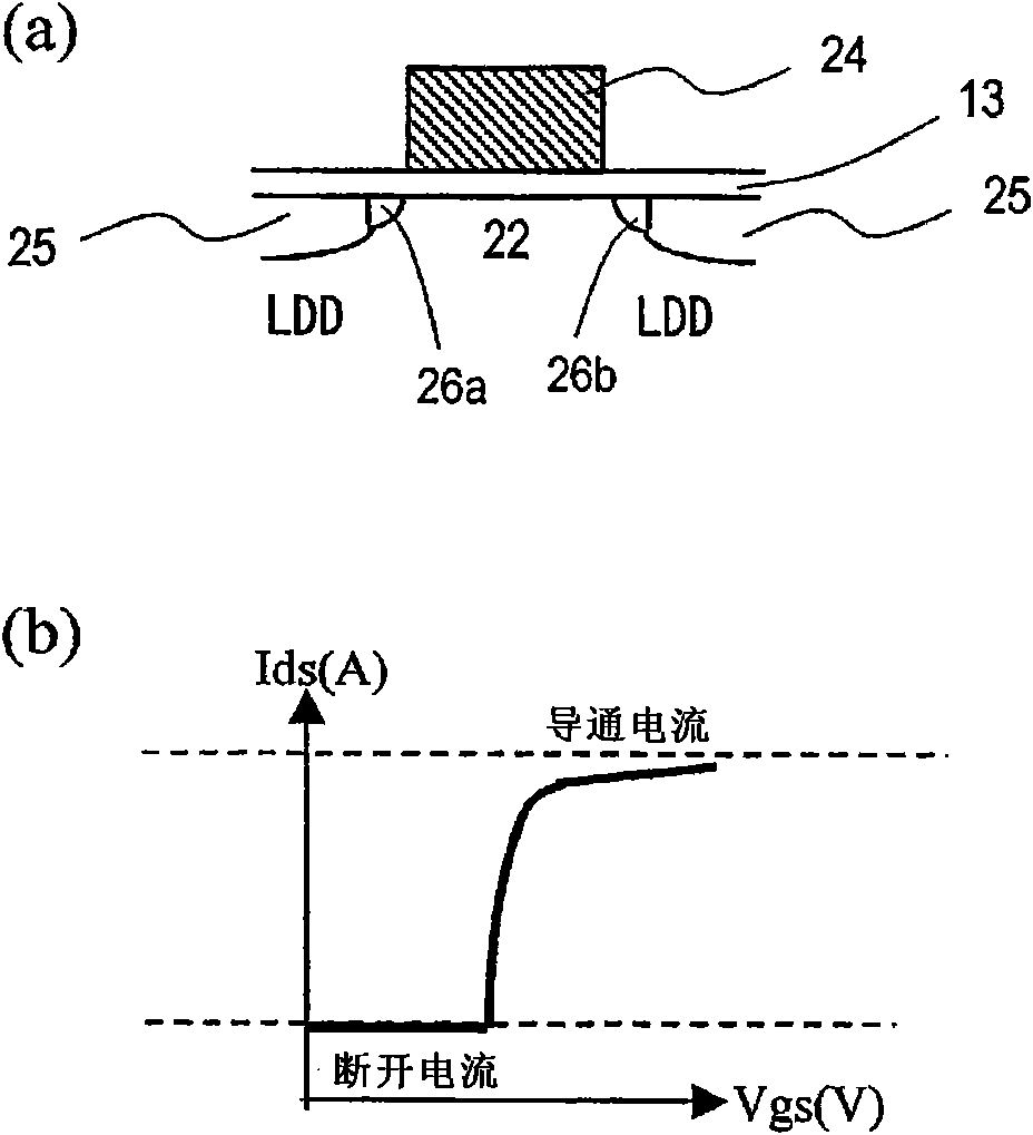
[0058] The semiconductor layer 10 has a channel region 12, a source / drain region (high concentration impurity region) 15, and LDD regions (low concentration impurity region) 16a and 16b having an impurity concentration lower than that of the source / drain region 15 . LDD regions 16 a and 16 b are formed between channel region ...

no. 2 approach

[0083] Hereinafter, a second embodiment of the semiconductor device of the present invention will be described with reference to the drawings. The semiconductor device of this embodiment has a structure in which two or more TFTs including a TFT with an LDD structure and a TFT with a GOLD structure are vertically stacked. "Vertical stacking" refers to a structure in which a source region of a TFT is connected to a drain region of another TFT. Here, a structure in which a single LDD structure TFT and a single GOLD structure TFT are stacked vertically (thin film transistor with a double gate structure) will be described as an example.

[0084] Image 6 is a cross-sectional view schematically showing the thin film transistor in this embodiment. For simplicity, in the same way as figure 1 The same reference numerals are attached to the same constituent elements of the thin film transistor 100 shown, and description thereof will be omitted.

[0085] The thin film transistor 200 ...

no. 3 approach

[0099] Hereinafter, a third embodiment of the semiconductor device of the present invention will be described with reference to the drawings. The thin film transistor of this embodiment mode includes reference figure 1 Vertically stacked structure of two TFTs in the structure described above.

[0100] Figure 8 is a cross-sectional view schematically showing the thin film transistor in this embodiment. For simplicity, in the same way as Image 6 The same constituent elements of the shown thin film transistor 200 are assigned the same reference numerals, and description thereof will be omitted.

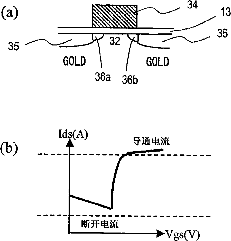
[0101] In the thin film transistor 300, the gate electrode 14A provided above the channel region 12A entirely overlaps with one of the LDD regions 16Aa and 16Ab located on both sides of the channel region 12A (GOLD structure), and overlaps with the LDD regions 16Aa and 16Ab. The other regions in do not overlap (LDD construction). Similarly, gate electrode 14B provided above channe...


PUM


Abstract

Provided is a semiconductor device wherein a gate electrode (14) of a thin film transistor (100) is formed of a single conductive film, and a semiconductor layer (10) is provided with a first low-concentration impurity region, which is arranged between the channel region (12) and the source region (15), and has an impurity concentration lower than the impurity concentrations of the source region and the drain region (15), and a second low-concentration impurity region, which is arranged between the channel region (12) and the drain region (15), and has an impurity concentration lower than the impurity concentrations of the source region and the drain region (15). A region (16a), which is one of the first and the second low-concentration impurity regions, entirely overlaps with the gate electrode (14), and a region (16b), which is the other one of the first and the second low-concentration impurity regions, does not overlap with the gate electrode (14).

Description

technical field [0001] The present invention relates to a semiconductor device and its manufacturing method. Background technique [0002] In recent years, liquid crystal display devices have been widely used due to advantages such as light weight, thin shape, and low power consumption. In particular, using an active matrix liquid crystal display device can increase the number of pixels and improve display contrast compared with a passive matrix liquid crystal display device, thereby enabling high-quality display. [0003] The active matrix liquid crystal display device includes a switching element such as a thin film transistor (Thin Film Transistor; hereinafter referred to as “TFT”) for each pixel. In this specification, the substrate on which the switching elements are formed is referred to as an "active matrix substrate". A typical active matrix liquid crystal display device includes an active matrix substrate, a counter substrate, and a liquid crystal layer provided t...

Claims


Application Information

Patent Timeline
Patent Type & Authority Applications(China)
IPC IPC(8): H01L21/336H01L29/423H01L29/49H01L29/786
CPCH01L29/78645H01L29/78621H01L29/78624H01L29/42384H01L29/78627
Inventor 庄司敦史中西勇夫堀田和重
Owner SHARP KK
Why Eureka
Try Eureka