Film coating device and method

A technology of coating device and holding tank, which is applied in the direction of sputtering plating, ion implantation plating, gaseous chemical plating, etc., and can solve the problems of affecting the electrical characteristics of semiconductor components and easily producing oxides, etc.

Inactive Publication Date: 2010-12-29
HONG FU JIN PRECISION IND (SHENZHEN) CO LTD +1
View PDF5 Cites 2 Cited by
  • Summary
  • Abstract
  • Description
  • Claims
  • Application Information

AI Technical Summary

Problems solved by technology

However, during the conversion process of the coating process, the surface of the semiconductor element is prone to oxides due to contact with air, which affects the electrical characteristics of the semiconductor element

Method used


Image

  • Film coating device and method
  • Film coating device and method
  • Film coating device and method

Examples


Embodiment Construction

[0016] The present invention will be further described in detail below in conjunction with the accompanying drawings.

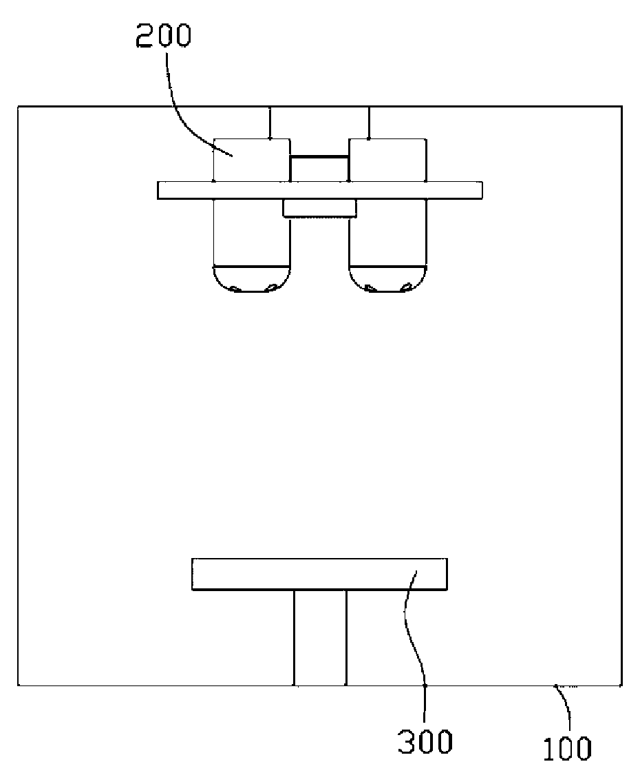
[0017] see figure 1 , a film coating device 10 , which includes a vacuum chamber 100 , a film coating source 200 and a workbench 300 . The vacuum chamber 100 can change the temperature and pressure inside it. The coating source 200 is disposed in the vacuum chamber 100 opposite to the workbench 300 . The workbench 300 is used to carry coating workpieces.

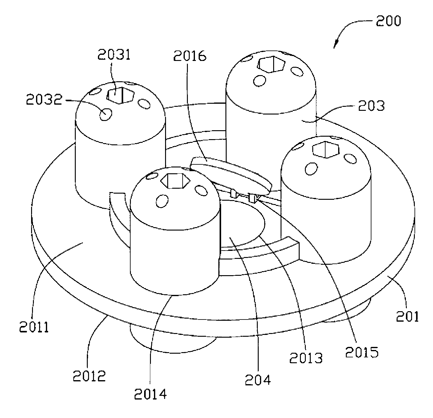
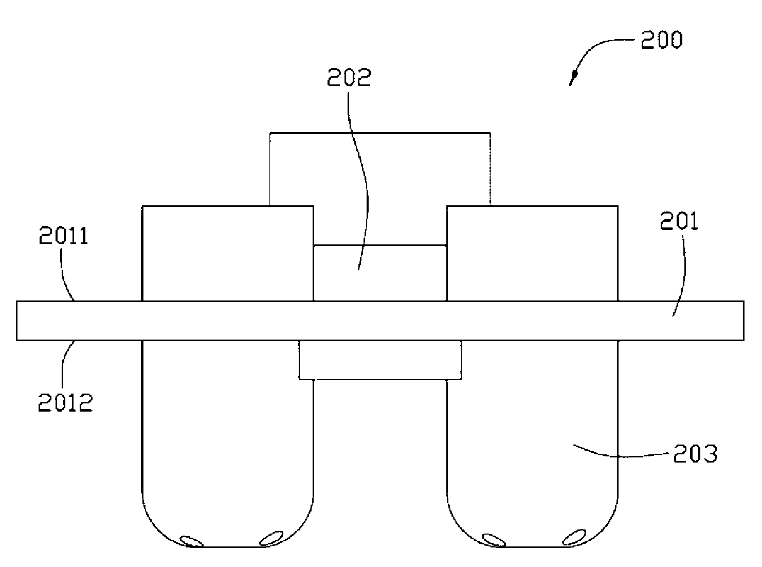
[0018] see figure 2 and image 3 , the coating source 200 includes a carrier 201 , a carrier shaft 202 , a plurality of airflow nozzles 203 and a target 204 . In this embodiment, the coating source 200 includes four airflow nozzles 203 .

[0019] The carrier 201 includes an upper surface 2011 and a lower surface 2012 , a receiving groove 2013 is disposed at the center of the upper surface 2011 , and a plurality of through holes 2014 are evenly formed around the receiving groove 2013 . In this embodi...


PUM


Abstract

The invention relates to a film coating device comprising a vacuum chamber, a film coating source and a work table, wherein the film coating source and the work table are oppositely arranged in the vacuum chamber; the film coating source comprises a bearing bracket, a plurality of airflow spray nozzles and a target material, wherein the target material is arranged on the bearing bracket, and the plurality of airflow spray nozzles are uniformly arranged on the bearing bracket around the target material. The film coating device is provided with the plurality of airflow spray nozzles and the target material, wherein the airflow spray nozzles are used for spraying reaction gases and realizing chemical vapor deposition film coating; and the target material is bombarded by high-energy ions and used for realizing physical vapor deposition. The film coating device can simultaneously carry out physical vapor deposition and chemical vapor deposition film coating processes. The invention also provides a film coating method.

Description

technical field [0001] The invention relates to a coating device and method. Background technique [0002] At present, coating methods generally include chemical vapor deposition methods and physical vapor deposition methods. For example, the metal connection layer of the semiconductor includes TiN, W, and AlCu layers, wherein the TiN and W layers are sprayed by chemical vapor deposition process, and the AlCu layer is sprayed by physical vapor deposition process. In the traditional process, the preparation of such semiconductor elements generally requires the conversion of physical and chemical coating processes. After one coating process is completed, it is necessary to break the vacuum to take out the object to be plated, and then move to the next coating process. However, during the conversion process of the coating process, the surface of the semiconductor element is prone to oxides due to contact with air, thereby affecting the electrical characteristics of the semicon...

Claims


Application Information

Patent Timeline
IPC IPC(8): C23C14/56C23C16/54C23C28/00
CPCC23C16/44C23C14/22
Inventor 裴绍凯
Owner HONG FU JIN PRECISION IND (SHENZHEN) CO LTD
Why Eureka
Try Eureka