

Asynchronous FIFO memory design with power of which the depth is not 2
A memory and deep technology, applied in the direction of instruments, calculations, special data processing applications, etc., can solve the problems of increased circuit area and power consumption, increased data output delay, etc.
- Summary
- Abstract
- Description
- Claims
- Application Information
AI Technical Summary
Problems solved by technology
Method used
Image

Examples
Embodiment Construction
[0010] The following content specifically describes the principle and an implementable solution of the present invention in practical application. The present invention is not limited to the applications and design solutions described below. Those who understand the field and have sufficient professional knowledge of circuit design can easily generalize and apply this patent to the design of other deep memories. The specific method of implementation may change the way of encoding, but the basic principle remains the same. In some drawings, numerals are used to help describe the principle of each part and the relationship between them.
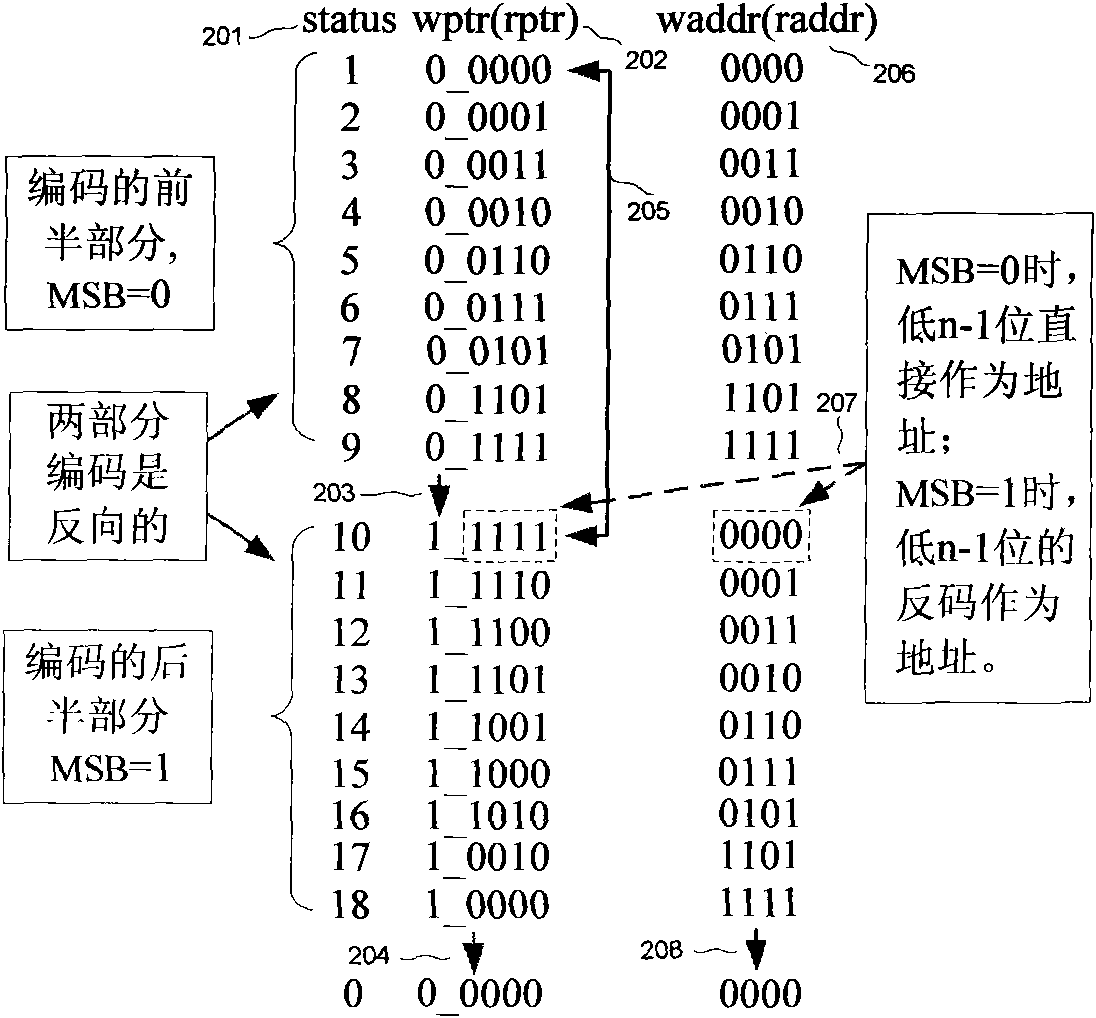
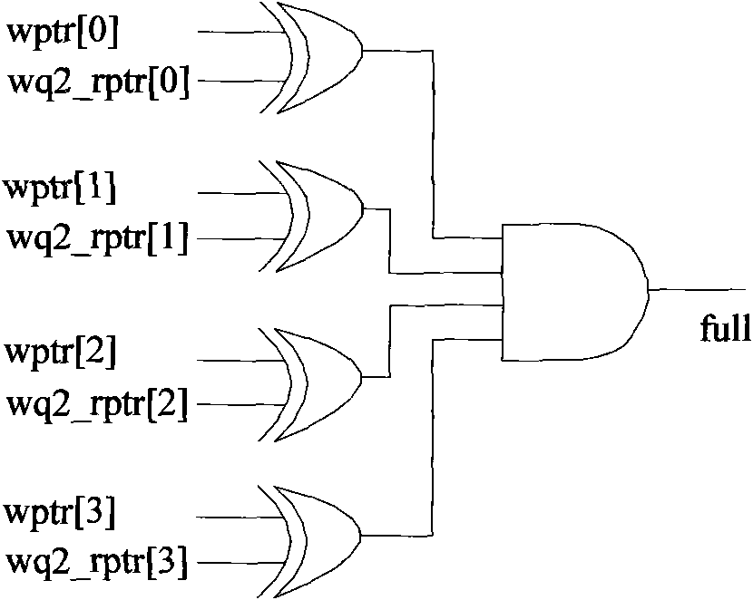
[0011] The content of the invention is mainly to use figure 2 The mentioned encoding designs asynchronous FIFO memories with a depth other than 2n, and image 3 and Figure 4 Circuit shown to generate empty / full signal.
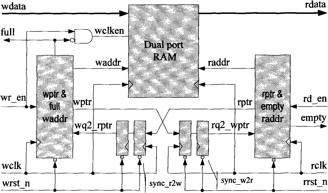
[0012] figure 1 Shown is the overall structure of the asynchronous FIFO. The whole system of asynchronous FIFO can be...
PUM
 Abstract
Description
Claims
Application Information