LED light-emitting module processing method

A technology of light-emitting modules and light-emitting diodes, which is applied in semiconductor/solid-state device manufacturing, electrical components, circuits, etc., can solve problems affecting light transmittance, light attenuation, and optical quality, and achieve the goal of increasing luminous flux and increasing light transmittance Effect

Inactive Publication Date: 2010-12-29
KWO GER METAL TECH +1
View PDF2 Cites 11 Cited by
  • Summary
  • Abstract
  • Description
  • Claims
  • Application Information

AI Technical Summary

Problems solved by technology

[0005] 1. The existing colloid E packaging is mainly used to protect the chip A and to transmit the light and heat generated by the chip A to the outside as much as possible. However, when the light generated by the chip A emits light and enters the lens F through the colloid E, the first Secondary refraction, and when the light passes through the lens F, it will produce double refraction, so some companies use colloid-free packaging, and directly use the lens F made of glass material as a jacket to protect the colloid E from aging and affecting light transmittance, etc. However, because there is a certain gap between the chip A and the lens F, the light will still cause refraction and light attenuation when passing through different air media.
[0006] 2. When the existing chip A is surface-mounted (SMT) with the preset circuit substrate, it needs to pass through a tin furnace at a high temperature of 250°C to 300°C, so that the colloid E will age when it is heated, and its heat resistance is not good, which is not conducive to the surface In addition to the adhesive welding operation, the overall optical quality of the lens F will also be slightly shrunk due to overheating, and the curvature will change, resulting in a decrease in the illumination of the bright light projected from the chip A towards the lens F, and a flat light source that emits uniform light outwards cannot be produced. Wait for the deletion to occur

Method used


Image

  • LED light-emitting module processing method
  • LED light-emitting module processing method
  • LED light-emitting module processing method

Examples


Embodiment Construction

[0033] In order to achieve the above-mentioned purpose and effect, the technical means and the structure adopted by the present invention are now illustrated in detail with respect to the preferred embodiments of the present invention. Its features and functions are as follows for complete understanding.

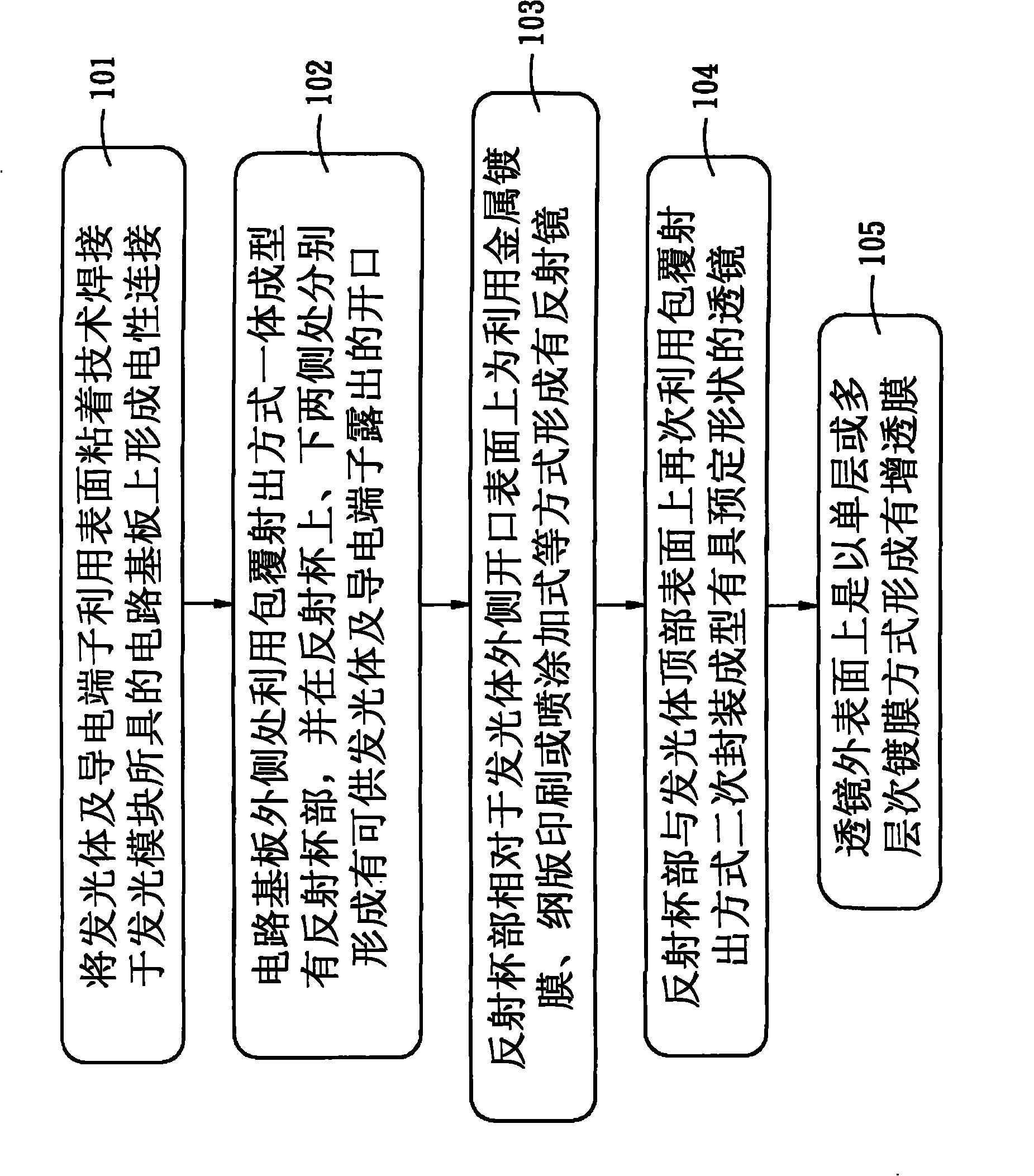
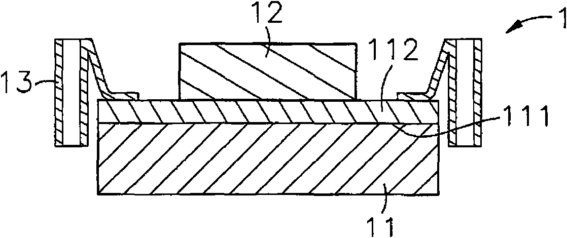
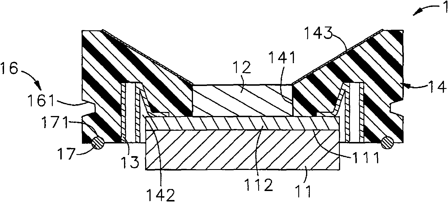
[0034] see Figure 1 to Figure 5 Shown are the manufacturing flow chart of the present invention, the side sectional view during welding, the side sectional view during injection molding, the side sectional view during secondary injection molding, and the three-dimensional appearance view after secondary injection molding, It can be clearly seen from the figure that the LED lighting module manufacturing method of the present invention includes the following steps for processing:

[0035] 101: Soldering: Solder at least one light emitting diode 12 and two or more conductive terminals 13 on the circuit substrate 11 of the light source module 1 by using surface mount technology...


PUM


Abstract

The invention relates to an LED light-emitting module processing method which comprises the steps of: respectively welding at least one LED and two or more conductive terminals on a circuit substrate of a light source module to form electrical connection, integrally forming an accommodating cup part outside the circuit substrate in a covering and ejecting mode and respectively forming openings for exposing the LEDs and the conductive terminals in the upper side and the lower side of the accommodating cup part; and carrying out secondary package on the surfaces of the tops of the accommodating cup part and the LEDs in a covering and ejecting mode to form a lens with preset shape, wherein the lens can be directly secondarily packaged and formed on the accommodating cup part and the LEDs to ensure that the inside of the lens does not have clearance so that the phenomena of refraction and light attenuation because lights passes through different media can be decreased for improving the intensity of illumination of the LEDs through projecting bright lights towards the lens and then being capable of ensuring that the light source module generates a planar light source uniformly and outwards emitting lights.

Description

technical field [0001] The invention relates to a process method of an LED light-emitting module, in particular, the lens can be encapsulated and molded on the surface of the container cup and the light-emitting diode by the method of coating injection, so that there is no gap inside, thereby reducing the number of light-emitting diodes. The method of refraction and light attenuation caused by light passing through different media. Background technique [0002] There are quite a lot of types of general lamps and the types of light they produce. Take the Light Emitting Diode (LED), which is common in the market and widely used in various fields, as an example. It not only has good photoelectric conversion efficiency, fixed wavelength, and light quantity , Adjustable light quality and other characteristics, and can achieve the advantages of small size, low heat generation and long service life, and it is more suitable for all kinds of downlights, headlights or table lamps and ...

Claims


Application Information

Patent Timeline
Patent Type & Authority Applications(China)
IPC IPC(8): H01L21/50H01L21/60H01L21/56H01L33/00
Inventor 林暄智
Owner KWO GER METAL TECH
Why Eureka
Try Eureka