Free curved surface micro-lens array device for photo-etching multi-pole illumination

A technology of microlens array and curved surface lens, which is applied in the field of lithography, can solve the problems of increasing system complexity, light beam entering the gap, reducing energy utilization rate, etc., and achieves the effect of wide application range, high energy utilization rate and small impact

Active Publication Date: 2011-01-05
ZHEJIANG UNIV
View PDF7 Cites 20 Cited by
  • Summary
  • Abstract
  • Description
  • Claims
  • Application Information

AI Technical Summary

Problems solved by technology

Since the tilt angle of each mirror on the two spatial beam modulators needs to be individually controlled by the control unit, this inevitably increases the complexity of the system
At the same time,

Method used


Image

  • Free curved surface micro-lens array device for photo-etching multi-pole illumination
  • Free curved surface micro-lens array device for photo-etching multi-pole illumination
  • Free curved surface micro-lens array device for photo-etching multi-pole illumination

Examples


Example Embodiment

[0076] Example 1

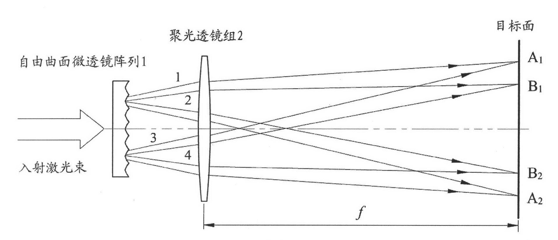
[0077] The dipole illumination mode is realized on the target surface by adopting the free-form surface micro-lens array device for lithography multipole illumination proposed by the present invention.

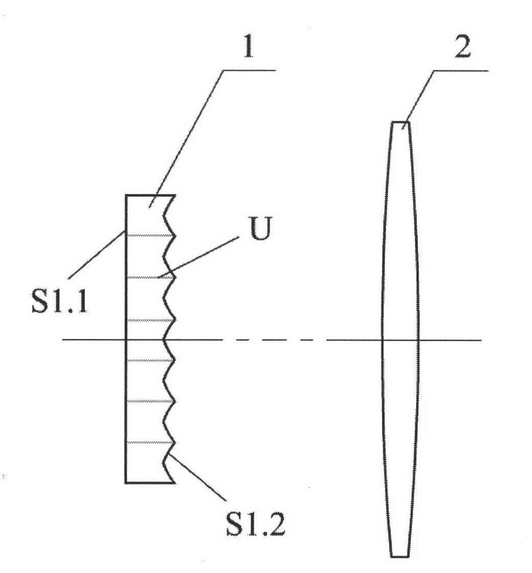
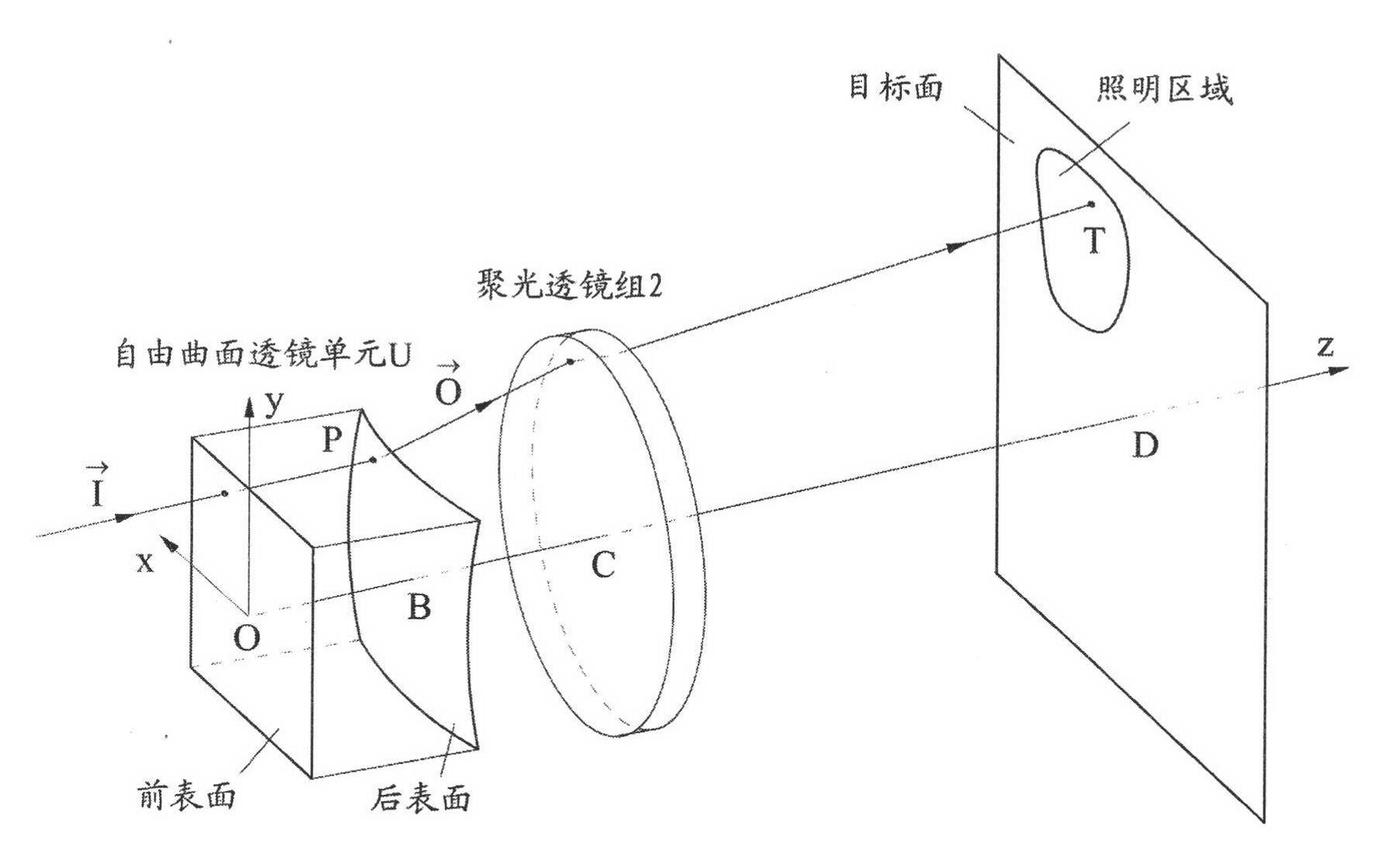
[0078] The cross-sectional shape of the free-form surface lens unit U perpendicular to the optical axis of the free-form surface micro-lens array for dipole illumination is rectangular, the front surface S2.1 of the free-form surface lens unit U is a plane, and the rear surface S2.2 is composed of the first The free-form surface S2.2.1 and the second free-form surface S2.2.2 are formed. exist Figure 4 middle, Figure 4 (a) is a cross-sectional view of the free-form surface lens unit U for realizing dipole illumination, Figure 4 (b) is the dipole illumination spot on the target surface. The first free-form surface S2.2.1 corresponds to the dipole illumination spot I on the target surface, and the second free-form surface S2.2.2 corresponds to the dipole...

Example Embodiment

[0095] Example 2

[0096] The quadrupole illumination mode is realized on the target surface by using the free-form surface microlens array device for lithography multipole illumination proposed by the present invention.

[0097] The free-form surface lens unit U of the free-form surface microlens array of quadrupole illumination has a rectangular cross-sectional shape perpendicular to the optical axis, the front surface S3.1 of the free-form surface lens unit U is a plane, and the rear surface S3.2 is formed by the first free-form surface S3. .2.1, the second free-form surface S3.2.2, the third free-form surface S3.2.3, the fourth free-form surface S3.2.4, the first plane S3.2.5, the second plane S3.2.6, the third plane S3.2.7 and the fourth Plane S3.2.8 constitutes. exist Figure 9 middle, Figure 9 (a) is a sectional view of the free-form surface lens unit U for realizing quadrupole illumination, Figure 9 (b) is the quadrupole illumination spot on the target surface. ...


PUM


Abstract

The invention discloses a free curved surface micro-lens array device for photo-etching multi-pole illumination. The device comprises a free curved surface micro-lens array 1 and a light-gathering lens group 2 which are arranged in turn along a light beam transmitting direction, wherein the free curved surface micro-lens array 1 consists of free curved surface lens units U which are uniformly distributed in lines and rows and have the same shape; the front surface S1.1 of the free curved surface micro-lens array 1 is a plane, while the back surface S1.2 is a free curved surface; the free curved surface micro-lens array 1 comprises a free curved surface micro-lens array for dipole illumination and a free curved surface micro-lens array for four-pole illumination; the light-gathering lens group 2 comprises at least one light-gathering lens; after being deflected by the free curved surface micro-lens array 1, light beams are imaged infinitely; and after being processed by the light-gathering lens group 2, outgoing light beams are imaged on the back focal plane of the light-gathering lens group 2. The device has the advantages of compact and simple structure, good reshaping effect, high energy utilization ratio, high practicability and wide application range.

Description

technical field [0001] The invention relates to the technical field of lithography, in particular to a free-form surface microlens array device used for lithography multipole illumination. Background technique [0002] With the development of semiconductor technology and the improvement of chip integration, the lithography process continues to move forward and repeatedly breaks the resolution limit. How to further improve the resolution and depth of focus of the projection lithography system and improve the performance of the projection lithography machine has become a Hot spots of attention. The purpose of improving the resolution can be achieved by shortening the exposure wavelength, increasing the numerical aperture of the projection objective, and reducing the process factor, but at the same time restricting the increase of the depth of focus. Using resolution enhancement technology is one of the main ways to solve the above problems. [0003] Off-axis illumination is ...

Claims


Application Information

Patent Timeline
IPC IPC(8): F21V5/04
Inventor 李海峰吴仍茂郑臻荣邢莎莎刘旭
Owner ZHEJIANG UNIV
Why Eureka
Try Eureka