TFT-LCD (Thin Film Transistor-Liquid Crystal Display) array substrate and manufacturing method thereof

An array substrate and semiconductor technology, which is applied in semiconductor/solid-state device manufacturing, optics, instruments, etc., can solve problems such as performance degradation of TFT-LCD array substrates, and achieve the effects of shortening production time, reducing contact resistance, and improving yield.

Inactive Publication Date: 2013-04-17
BOE TECH GRP CO LTD +1
View PDF2 Cites 0 Cited by
  • Summary
  • Abstract
  • Description
  • Claims
  • Application Information

AI Technical Summary

Problems solved by technology

[0005] The purpose of the present invention is to provide a method for manufacturing a TFT-LCD array substrate, which effectively solves the technical defect of the prior art that the performance of the TFT-LCD array substrate is reduced due to the use of a thicker semiconductor film

Method used


Image

  • TFT-LCD (Thin Film Transistor-Liquid Crystal Display) array substrate and manufacturing method thereof
  • TFT-LCD (Thin Film Transistor-Liquid Crystal Display) array substrate and manufacturing method thereof
  • TFT-LCD (Thin Film Transistor-Liquid Crystal Display) array substrate and manufacturing method thereof

Examples


Embodiment Construction

[0059] The technical solutions of the present invention will be described in further detail below with reference to the accompanying drawings and embodiments.

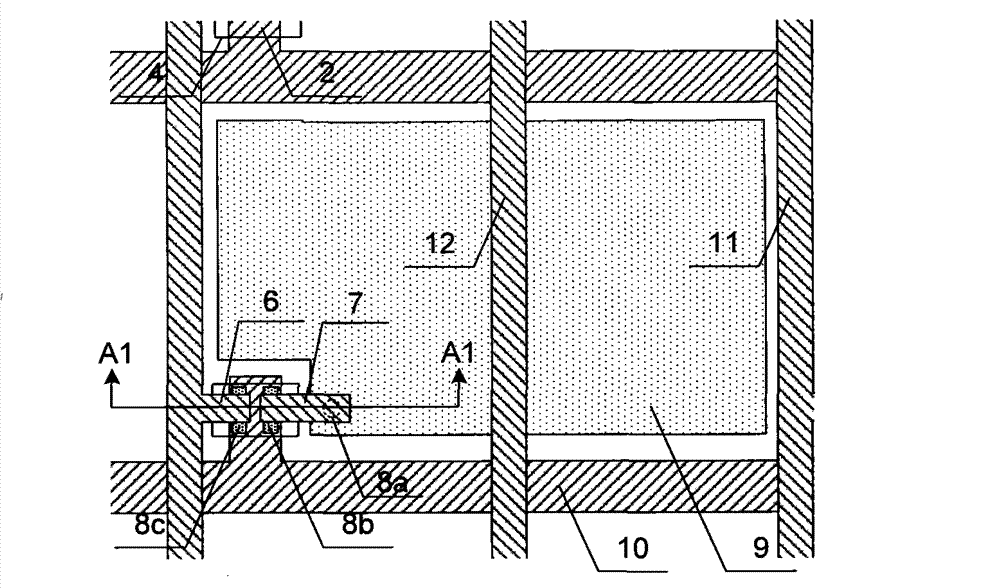
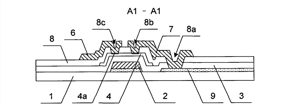
[0060] figure 1 It is a plan view of the first embodiment of the TFT-LCD array substrate of the present invention, figure 2 for figure 1 Sectional view of A1-A1 in the middle. Such as figure 1 with figure 2 As shown, the main structure of the TFT-LCD array substrate in this embodiment includes gate lines 10, data lines 11, common electrode lines 12, pixel electrodes 9 and thin film transistors, and the gate lines 10 and data lines 11 perpendicular to each other define pixel areas. The thin film transistor and the pixel electrode 9 are formed in the pixel area, the gate line 10 is used to provide the turn-on signal to the thin film transistor, the data line 11 is used to provide the data signal to the pixel electrode 9, and the common electrode line 12 is used to form a storage capacitor with the pixel electrode 9...


PUM


Abstract

A thin film transistor liquid crystal display (TFT-LCD) array substrate comprises a gate line, a data line, a pixel electrode and a thin film transistor. The pixel electrode and the thin film transistor are formed in a pixel region defined by intersecting of the gate line and the data line, and the thin film transistor comprises a gate electrode, a semiconductor layer, a source electrode and a drain electrode. Two separate parts of the surface of the semiconductor layer are treated by a surface treatment to form into an ohmic contact layer, and the source electrode and the drain electrode are connected with the semiconductor layer through the ohmic contact layer in the two separate parts, respectively.

Description

technical field [0001] The invention relates to a liquid crystal display and a manufacturing method thereof, in particular to a TFT-LCD array substrate and a manufacturing method thereof. Background technique [0002] Thin Film Transistor Liquid Crystal Display (TFT-LCD for short) has the characteristics of small size, low power consumption, and no radiation, and occupies a dominant position in the current flat panel display market. For TFT-LCD, the array substrate and manufacturing process determine its product performance, yield and price. In order to effectively reduce the price and increase the yield, the manufacturing process of the TFT-LCD array substrate has been gradually simplified, from the initial seven patterning (7mask) process to the four patterning (4mask) based on halftone or gray tone mask technology. ) process. [0003] At present, the manufacture of the TFT-LCD array substrate is completed by forming a thin film pattern through a group of patterning proc...

Claims


Application Information

Patent Timeline
Patent Type & Authority Patents(China)
IPC IPC(8): G02F1/1362G02F1/1368H01L21/82
CPCH01L27/1214H01L27/1288H01L29/66765H01L29/4908H01L29/78618G02F2001/136295G02F1/136295G02F1/136286G02F1/1368G02F1/136236H01L21/0271H01L21/31111H01L21/31133
Inventor 刘翔谢振宇陈旭
Owner BOE TECH GRP CO LTD
Why Eureka
Try Eureka